Service Manuals, User Guides, Schematic Diagrams or docs for : . Electronic Components Datasheets Various datasheets 80c51_fam_prog_guide_1

<< Back | Home

Most service manuals and schematics are PDF files, so You will need Adobre Acrobat Reader to view : Acrobat Download Some of the files are DjVu format. Readers and resources available here : DjVu Resources
For the compressed files, most common are zip and rar. Please, extract files with Your favorite compression software ( WinZip, WinRAR ... ) before viewing. If a document has multiple parts, You should download all, before extracting.
Good luck. Repair on Your own risk. Make sure You know what You are doing.


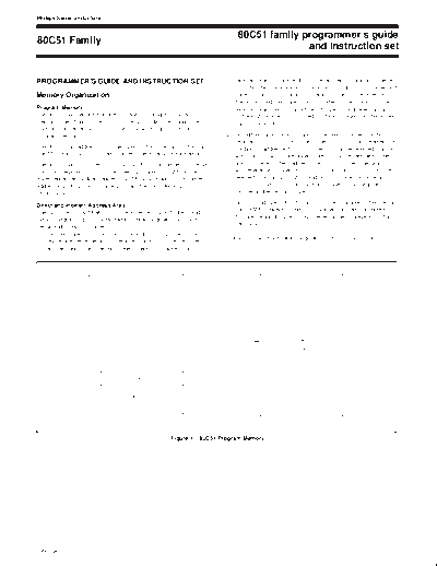
Image preview - the first page of the document
80c51_fam_prog_guide_1


>> Download 80c51_fam_prog_guide_1 documenatation <<

Text preview - extract from the document
Philips Semiconductors


                                                                                 80C51 family programmer's guide
80C51 Family
                                                                                               and instruction set


PROGRAMMER'S GUIDE AND INSTRUCTION SET                                        register bank contains eight 1-byte registers 0 through 7. Reset
                                                                              initializes the stack pointer to location 07H, and it is incremented
Memory Organization                                                           once to start from location 08H, which is the first register (R0) of
                                                                              the second register bank. Thus, in order to use more than one
Program Memory                                                                register bank, the SP should be initialized to a different location
The 80C51 has separate address spaces for program and data                    of the RAM where it is not used for data storage (i.e., the higher
memory. The Program memory can be up to 64k bytes long. The                   part of the RAM).
lower 4k can reside on-chip. Figure 1 shows a map of the 80C51
program memory.                                                            2. Bit Addressable Area: 16 bytes have been assigned for this
                                                                              segment, 20H-2FH. Each one of the 128 bits of this segment can
The 80C51 can address up to 64k bytes of data memory to the chip.             be directly addressed (0-7FH). The bits can be referred to in two
The MOVX instruction is used to access the external data memory.              ways, both of which are acceptable by most assemblers. One
The 80C51 has 128 bytes of on-chip RAM, plus a number of Special              way is to refer to their address (i.e., 0-7FH). The other way is
Function Registers (SFRs). The lower 128 bytes of RAM can be                  with reference to bytes 20H to 2FH. Thus, bits 0-7 can also be
accessed either by direct addressing (MOV data addr) or by indirect           referred to as bits 20.0-20.7, and bits 8-FH are the same as
addressing (MOV @Ri). Figure 2 shows the Data Memory                          21.0-21.7, and so on. Each of the 16 bytes in this segment can
organization.                                                                 also be addressed as a byte.
                                                                           3. Scratch Pad Area: 30H through 7FH are available to the user as
Direct and Indirect Address Area
                                                                              data RAM. However, if the stack pointer has been initialized to
The 128 bytes of RAM which can be accessed by both direct and
                                                                              this area, enough bytes should be left aside to prevent SP data
indirect addressing can be divided into three segments as listed
                                                                              destruction.
below and shown in Figure 3.
1. Register Banks 0-3: Locations 0 through 1FH (32 bytes). The
                                                                           Figure 2 shows the different segments of the on-chip RAM.
    device after reset defaults to register bank 0. To use the other
    register banks, the user must select them in software. Each


                   FFFF                                                           FFFF


                                         60k
                                        BYTES
                                      EXTERNAL


                                                                            OR                          64k
                                                                                                       BYTES
                                                                                                     EXTERNAL


                   1000

                                          AND
                   0FFF

                                        4k BYTES
                                       INTERNAL

                   0000                                                           0000


                                                                                                                    SU00567

                                                       Figure 1. 80C51 Program Memory


1997 Sep 18                                                            1
Philips Semiconductors

                                                                        80C51 family programmer's guide
80C51 Family
                                                                                       and instruction set


                                                                       0FFF


                               INTERNAL


                   FF
                                                                                           64k
                                                                                          BYTES
                                SFRs                                                    EXTERNAL
                         DIRECT ADDRESSING
                                ONLY

                   80
                                                                 AND

                   7F
                         DRIECT AND INDIRECT
                             ADDRESSING


                   00                                                  0000


                                                                                                        SU00568

                                               Figure 2. 80C51 Data Memory


                                                   8 BYTES


                         78                                                            7F

                         70                                                            77

                         68                                                            6F

                         60                                                            67

                         58                                                            5F    SCRATCH
                                                                                               PAD
                         50                                                            57     AREA

                         48                                                            4F

                         40                                                            47

                         38                                                            3F

                         30                                                            37

                         28                                                   ... 7F   2F       BIT
                                                                                            ADDRESSABLE
                         20   0 ...                                                    27     SEGMENT

                         18                            3                               1F

                         10                            2                               17    REGISTER
                                                                                              BANKS
                         08                            1                               0F

                         00                            0                               07


                                                                                               SU00569

                                Figure 3. 128 Bytes of RAM Direct and Indirect Addressable


1997 Sep 18                                                  2
Philips Semiconductors

                                                                             80C51 family programmer's guide
80C51 Family
                                                                                            and instruction set


Table 1.       80C51 Special Function Registers
                                     DIRECT       BIT ADDRESS, SYMBOL, OR ALTERNATIVE PORT FUNCTION
 SYMBOL          DESCRIPTION                                                                                     RESET VALUE
                                    ADDRESS      MSB                                              LSB
 ACC*         Accumulator              E0H         E7      E6         E5    E4       E3       E2     E1    E0        00H
 B*           B register               F0H         F7      F6         F5    F4       F3       F2     F1    F0        00H
 DPTR         Data pointer (2 by-
              tes)
   DPH        Data pointer high        83H                                                                           00H
   DPL        Data pointer low         82H                                                                           00H
                                                   AF      AE         AD    AC       AB      AA      A9    A8
 IE*          Interrupt enable         A8H         EA       


◦ Jabse Service Manual Search 2024 ◦ Jabse PravopisonTap.bg ◦ Other service manual resources online : FixyaeServiceinfo