Service Manuals, User Guides, Schematic Diagrams or docs for : . Electronic Components Datasheets Various icservice
<< Back | HomeMost service manuals and schematics are PDF files, so You will need Adobre Acrobat Reader to view : Acrobat Download Some of the files are DjVu format. Readers and resources available here : DjVu Resources
For the compressed files, most common are zip and rar. Please, extract files with Your favorite compression software ( WinZip, WinRAR ... ) before viewing. If a document has multiple parts, You should download all, before extracting.
Good luck. Repair on Your own risk. Make sure You know what You are doing.
Image preview - the first page of the document
>> Download icservice documenatation <<
Text preview - extract from the document
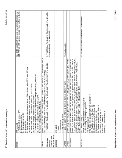
IC Service "first aid" information examples                                                                                                       1  34


24CO8           PIN VALUE                                                                                     Is a 8Kbit electrically erasable programmable memory
                1. Write protect enable :0V                                                                   (EEPROM), with a power supply value as low as 2.5V.
                2. Not connected :0V
                3. Chip enable input :0V
                4. Ground :0V
                5. Serial data address input/output :Input LOW voltage: Min:-0.3V, Max:0.3*Vcc
                :Input HIGH voltage: Min:0.7*Vcc, Max:Vcc+1
                6. Serial clock :Input LOW voltage: Min:-0.3V, Max:0.3*Vcc
                :Input HIGH voltage: Min:0.7*Vcc, Max:Vcc+1
                7. Multibyte/Page write mode :Input LOW voltage: Min:-0.3V, Max:0.5V
                :Input HIGH voltage: Min:Vcc-0.5, Max:Vcc+1
                8. Supply voltage :Min:2.5V, Max:5.5V
CNR50           pin1 = -, pin2 = 0,9V (1,4V standby), pin3 = -, pin4 = -, pin5 = 4,6V (-0,7V standby), pin6 =
                -3V (-0,5V standby), pin7 = -1V (2V8 standby), pin8 = 13,1V (5,5V standby).
Differences     1. TDA8362 : Pin 9=GND, Pin 41=VFB, Pin 42=VRAMP, Pin 43=VOUT, Pin 44=AFC                     2. TDA8362A :Pin 9=AFC, Pin 41=GND, Pin 42=VFB,
between                                                                                                       Pin 43=VRAMP, Pin 44=VOUT
TDA8362 and
the TDA8362A
G1965M          PINNING
                1. Input
                2. Input-ground
                3. Chip carrier-ground
LA7830          1. GND, 2. 13.5V, 3. 25,8V, 4. 0.9V, 5. 0.8V, 6. 25,3V, 7. 1,6V                            Vertical amplifier
LA7830          pin1 = 0V, pin2 = 13,8V, pin3 = 24,1V, pin4 = 1,35V, pin5 = 0V, pin6 = 23,6V, pin7 = 0,6V
M51354AP        pin1 = 3,9V, pin2 = 4,4V, pin3 = 4,4V, pin4 = 12,1V, pin5 = 0,02V, pin6 = 0V, pin7 = 4,1V,
                pin8 = 4,1V, pin9 = 4,1V, pin10 = 4,1V, pin11 = 0V, pin12 = 5,0V, pin13 = 11,6V, pin14 =
                7,0V, pin15 = 5,0V, pin16 = 6,4V, pin17 = 4,7V, pin18 = 4,6V, pin19 = 4,6V, pin20 = 5,8V,
                pin21 = 4,2V, pin22 = 2,8V, pin23 = 2,8V, pin24 = 6,0V, pin25 = 0,48V, pin26 = 6,0V,
                pin27 = 6,0V, pin28 = 0,72V, pin29 = 4,6V, pin30 = 5,8V
M62501P         VCC Power supply 2                                                                         IC for the synchronized deflection system control
                VREF Output of reference voltage (5V) 15
                COSC Setting oscillating frequency 4
                TIN Trigger input 3
                DTC Dead time control (Soft start function) 14
                IN+ Positive input of Op-Amp. 11
                IN- Negative input of Op-Amp. 12
                FB Output of Op-Amp. 13
                BI Positive input of buffer Amp. 9
                BO Output of buffer Amp. 10
                CAGC AGC setting 5
                PWM OUT PWM output 1


http://www.tehnicaavtv.com/icservice.htm                                                                                                               21/11/2002
IC Service "first aid" information examples                                                                        2  34


                P.OUT Error signal output 6
                OVP Input of over voltage protection 7
                UVP Input of under voltage protection 8
                GND Ground 16
MC44604         PIN VALUE
                1. Output Supply Voltage (Vcc) : 12VDC
                2. Output Supply Voltage (Vc) : 12VDC
                3. Output voltage : LOW Level Drop Voltage 1VDC, Max : 1.2VDC (Isink=100mA)
                1.4VDC, Max : 2VDC (Isink=500mA)
                HIGH Level Drop Voltage 1.5VDC, Max : 2VDC (Isource=200mA)
                2VDC, Max : 2.7VDC (Isource=500mA)
                4. Ground
                5. Fold back input: 0.9VDC, Min:-0.3VDC, Max : Vcc+0.3VDC
                6. Over voltage protection (OVP) : 0.78VDC, Min:-0.3VDC, Max : Vcc+0.3VDC
                7. Current sense input: Min:-0.3VDC, Max : Vcc+0.3VDC
                8. Demagnetization detection input : Idemag-ib (source):-4mA Idemag-ib (sink) : 10mA
                9. Standby current set: Ipeak-stby/Iref : 0.40 Min : 0.37 Max : 0.43
                10. Oscillator voltage swing: 2Vpp
                11. Soft start/Dmax/Voltage mode: Idischarge : 5mA, Min : 1.5mA (Vsoft start=1V)
                12. Clamp E/A input: 4.7VDC, Min : 4.5VDC Max : 4.9VDC
                13. E/A output: HIGH State: 6.5VDC, Min : 5.5VDC, Max : 7.5VDC LOW State : 1.0VDC,
                1.1VDC
                14. E/A input: 2.5VDC, Min : 2.4VDC, Max : 2.6VDC
                15. Stand-by management: Stand-by On Detection current ratio : Idet/Iref : 0.38, Min :
                0.34, Max : 0.42
                Stand-by regulation current ratio : Ireg/Iref : 20.5, Min : 18, Max : 23
                16. Rref input: 2.5VDC, Min : 2.4VDC, Max : 2.6VDC
MC44605         Pin 1 V CC This pin is the positive supply of the IC.
                Pin 2 V C The output high state, V OH, is set by the voltage applied to this pin. With a
                separate connection to the power source, it gives the possibility to set by means of an
                external resistor the output source current at a different value than the sink current.
                Pin 3 Output The output current capability is suited for driving a power MOSFET.
                Pin 4 GND The ground pin is a single return typically connected back to the power source.
                It is used as control and power ground.
                Pin 5 Maximum Power Limitation This block enables to estimate the input power. When
                this calculated power is detected as too high, fault information is sent to the disabling block
                in order to definitively disable the circuit.
                Pin 6 Over
◦ Jabse Service Manual Search 2026 ◦ Jabse Pravopis ◦ onTap.bg ◦ Other service manual resources online : Fixya ◦ eServiceinfo