Service Manuals, User Guides, Schematic Diagrams or docs for : . Electronic Components Datasheets Various rt9199

<< Back | Home

Most service manuals and schematics are PDF files, so You will need Adobre Acrobat Reader to view : Acrobat Download Some of the files are DjVu format. Readers and resources available here : DjVu Resources
For the compressed files, most common are zip and rar. Please, extract files with Your favorite compression software ( WinZip, WinRAR ... ) before viewing. If a document has multiple parts, You should download all, before extracting.
Good luck. Repair on Your own risk. Make sure You know what You are doing.


Image preview - the first page of the document
rt9199


>> Download rt9199 documenatation <<

Text preview - extract from the document
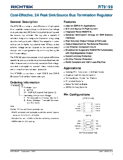
                                                                                                          RT9199

Cost-Effective, 2A Peak Sink/Source Bus Termination Regulator
General Description                                                Features
The RT9199 is a simple, cost-effective and high-speed               Ideal for DDR-II VTT Applications
linear regulator designed to generate termination voltage           Sink and Source 2A Peak Current
in double data rate (DDR) memory system to comply with              Integrated Power MOSFETs
the devices requirements. The regulator is capable of               Generate Termination Voltage for DDR Memory
actively sinking or sourcing up to 2A peak while regulating         Interfaces
an output voltage to within 20mV. The output termination            High Accuracy Output Voltage at Full-Load
voltage can be tightly regulated to track 1/2VDDQ by two            Output Adjustment by Two External Resistors
external voltage divider resistors or the desired output            Low External Component Count
voltage can be pro-grammed by externally forcing the                Shutdown for Suspend to RAM (STR) Functionality
REFEN pin voltage.                                                  with High-Impedance Output
                                                                    Current Limiting Protection
The RT9199 also incorporates a high-speed differential
                                                                    On-Chip Thermal Protection
amplifier to provide ultra-fast response in line/load transient.
                                                                    RoHS Compliant and 100% Lead (Pb)-Free
Other features include extremely low initial offset voltage,
excellent load regulation, current limiting in bi-directions
and on-chip thermal shut-down protection.                          Applications
                                                                    Desktop PCs, Notebooks, and Workstations
The RT9199 are available in both SOP-8 and SOP-8
                                                                    Graphics Card Memory Termination
(Exposed Pad) surface mount packages.
                                                                    Set Top Boxes, Digital TVs, Printers
                                                                    Embedded Systems
Ordering Information
                                                                    Active Termination Buses
RT9199
                 Package Type                                       DDR/II Memory Systems
                 S : SOP-8
                 SP : SOP-8 (Exposed Pad-Option 2)
                 Operating Temperature Range                       Pin Configurations
                 P : Pb Free with Commercial Standard                                  (TOP VIEW)
                 G : Green (Halogen Free with Commer-
                     cial Standard)
                                                                                 VIN                8   VCNTL
Note :                                                                          GND     2           7   VCNTL
                                                                              REFEN     3           6   VCNTL
Richtek Pb-free and Green products are :
                                                                               VOUT     4           5   VCNTL
  RoHS compliant and compatible with the current require-
   ments of IPC/JEDEC J-STD-020.                                                            SOP-8
  Suitable for use in SnPb or Pb-free soldering processes.
  100%matte tin (Sn) plating.                                                   VIN                 8   NC
                                                                               GND      2           7   NC
                                                                                          GND
                                                                             REFEN      3      6        VCNTL
                                                                                             9
                                                                              VOUT      4      5        NC

                                                                                  SOP-8 (Exposed Pad)


DS9199-07     September 2007                                                                                 www.richtek.com
                                                                                                                           1
RT9199
Typical Application Circuit

             VCNTL = 5V

                  VIN = 1.8V
                                                                                                                       RTT

                                              R1                    VIN        VCNTL              CIN     CCNTL
                                                                      RT9199
                                                                 REFEN       VOUT
                               2N7002
                         EN                               CSS
                                              R2                          GND
                                                                                                        COUT RDUMMY


             R1 = R2 = 100k, RTT = 50 / 33 / 25
             COUT(MIN) = 10F (Ceramic) + 1000F under the worst case testing condition
             RDUMMY = 1k as for VOUT discharge when VIN is not presented but VCNTL is presented
             CSS = 1F, CIN = 470F (Low ESR), CCNTL = 47F


Test Circuit

                                              VIN = 1.8V         VCNTL = 5V


                                                   VIN          VCNTL
                                                   RT9199                              VOUT
                                   1.25V      REFEN       VOUT

                                                         GND                             COUT       V
                                                                                 IL


                                             Figure 1. Output Voltage Tolerance, VLOAD


                                                         VCNTL = 5V
                     VIN = 1.8V     A

                                             VIN         VCNTL
                                                RT9199                                       0.9V
                                                                                 VOUT
                          0.9V             REFEN       VOUT
                                                                                                    0V
                                                   GND                                COUT
                          0.15V                                           RL                  V


                                                                                                         RL and COUT
                                                                                                         Time deleay

                                             Figure 2. Current in Shutdown Mode, ISTBY


www.richtek.com                                                                                            DS9199-07    September 2007
2
                                                                                                                  RT9199

                                              VIN = 1.8V         VCNTL = 5V


                                                   VIN       VCNTL
                                                   RT9199                                VOUT
                               0.9V           REFEN       VOUT

                                                         GND                   A           COUT    V
                                                                                   IL


                                              Figure 3. Current Limit for High Side, ILIM


                                 Power Supply                  VCNTL = 5V
                                with Current Limit
                                         VIN = 1.8V
                                                                                A
                                                   VIN         VCNTL
                                                                                    IL
                                                     RT9199                               VOUT
                                0.9V            REFEN       VOUT

                                                           GND                              COUT   V


                                              Figure 4. Current Limit for Low Side, ILIM


                                                                             VCNTL = 5V
                                 VIN = 1.8V


                                                                 VIN        VCNTL
                                                                  RT9199                           VOUT
                        0.9V                                 REFEN       VOUT
                   VREFEN
                             0.15V                                     GND                  RL         COUT
                                                                                                              V
                        0.9V

                     VOUT
                               0V
                                                         VOUT would be low if VREFEN < 0.15V
                                                         VOUT would be high if VREFEN > 0.6V

                                     RL and COUT
                                     Time deleay


                                       Figure 5. REFEN Pin Shutdown Threshold, VIH & VIL


DS9199-07   September 2007                                                                                        www.richtek.com
                                                                                                                                3
RT9199
Functional Pin Description
VIN
Input voltage which supplies current to the output pin. Connect this pin to a well-decoupled supply voltage. To prevent the
input rail from dropping during large load transient, a large, low ESR capacitor is recommended to use. The capacitor
should be placed as close as possible to the VIN pin.

GND (Exposed Pad)
Common Ground. The exposed pad must be soldered to a large PCB and connected to GND for maximum power
dissipation.

VCNTL
VCNTL supplies the internal control circuitry and provides the drive voltage. The driving capability of output current is
proportioned to the VCNTL. Connect this pin to 5V bias supply to handle large output current with at least 1F capacitor
from this pin to GND. An important note is that VIN should be kept lower or equal to VCNTL.

REFEN
Reference voltage input and active low shutdown control pin. Two resistors dividing down the VIN voltage on the pin to
create the regulated output voltage. Pulling the pin to ground turns off the device by an open-drain, such as 2N7002,
signal N-MOSFET.

VOUT
Regulator output. VOUT is regulated to REFEN voltage that is used to terminate the bus resistors. It is capable of sinking
and sourcing current while regulating the output rail. To maintain adequate large signal transient response, typical value
of 1000F Al electrolytic capacitor with 10F ceramic capacitors are recommended to reduce the effects of current
transients on VOUT.


Function Block Diagram
                                                       VCNTL            VIN


                                                    Current Limit
                                                  Thermal Protection


                                                        +
                               REFEN
                                                             EA                       VOUT
                                                         -


                                                                  GND


www.richtek.com                                                                              DS9199-07    September 2007
4
                                                                                                                          RT9199
Absolute Maximum Ratings                             (Note 1)
 Input Voltage, VIN ------------------------------------------------------------------------------------------------------ 6V
 Control Voltage, VCNTL ----------------------------------------------------------------------------------------------- 6V
 Power Dissipation, PD @ TA = 25


◦ Jabse Service Manual Search 2024 ◦ Jabse PravopisonTap.bg ◦ Other service manual resources online : FixyaeServiceinfo