Service Manuals, User Guides, Schematic Diagrams or docs for : . Rare and Ancient Equipment B&K 1477 Service Manual
<< Back | HomeMost service manuals and schematics are PDF files, so You will need Adobre Acrobat Reader to view : Acrobat Download Some of the files are DjVu format. Readers and resources available here : DjVu Resources
For the compressed files, most common are zip and rar. Please, extract files with Your favorite compression software ( WinZip, WinRAR ... ) before viewing. If a document has multiple parts, You should download all, before extracting.
Good luck. Repair on Your own risk. Make sure You know what You are doing.
Image preview - the first page of the document
>> Download 1477 Service Manual documenatation <<
Text preview - extract from the document
jrfo Bi(F#C!S#J
\,\
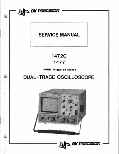
MANUAL
SERVICE
1472C
1477
lSMHz Triggered Sweep
DUAL-TRAGE
OSqLLOSCOPE
lllronn' Bt(
\,\
WARilI1{G
fhis service mantrcrl is intended for use W qnlified electronics
teclnicions only. To arrcid electnc shock, do not perf orm servrcrng urless
yvu are qnlified to do so.
High voltage up to 2000 rfDC is present on the CRT and power supply
board when tJle oscilloscope is operating. High voltage up to f95 VDC is
present on the sweep board. Line voltage of LZO VAC (or 240 VAC) is
present on the power transformer, on-off switch, and power supply board
any time the oscilloscope is corurected to:ur AC power source, even if
turned off. Always observe caution when the housing is removed from the
unit. Contacting exposed high voltage could result in fatal electric shock.
\-
DIFFERENCE-S BETWEEN MODELS
This second edition of the service manual is expanded to include Model
t477. Electricaly, Model 1477 is very similar to the Model 1472C. A sep-
arate schematic is supplied for eadr model. The circuit board drawings
essentially apply to both models. Model L477 has several changes in ap-
pearzrnce from Model l47ZC, using a new front panel, new handle, new
knobs, etc. A parts list itemizing those parts which are unique for Model
1477 is on page 34.
\-
TABLE OF CONTENTS
b OPERATOR'SCONTROLS'INDICATORS AND FACILITIES . . . . . . . . . . 3
S P E C I F I C A T I O N S . . . . . . . . . . . .. .. .. . . . . . . . . . . o o . . . . . . . . . . . 5
o
C I R C U I T D E S C R I P T I O N . . . . . . . . . . . . . f. .. .. .. . . o . . . . . . . . . . . . 7
S E R V I C I N. G . . . . . . . . .
. r . . . . . . . . . . o . . . . . . . . . . . . . . . o o . . . . . 8
TROUBLESHOOTING . . . . . . . . . . . . . . . . . . . . . . . . . . . . . . . . . . . . . 10
AD JU STMENTS . . . . . . . . . . . . . . . . . . . . . . . . . . . . . . . . . . . . . . . . . 16
P A R T SL f S T . . . . . . . . . . . . . . . . . . . . . . . . o . o . . . . . . . r r I r . . . . . , Z !
CIRCUIT BOARD MAPS
PowerSuppIy.................................... .27
V e r t i c a lm p l i f i e rr . . . . . . . . . . . . . . . .
A . '............. ... 28
S w e e p B o a r d. . . . . . . . . . . . . . o o . . . . . . . . o . o . o o o . . r . . . . . 2 g
VO LTAGE M EASUREM ENTS . . o . . . . . . . . . . . . . . . . . . . . . . . . . . . . . 30
MODEL I4TZCPRODUCTION CHANGES. . . . . . . o . . o . . . . . . . . . . . . 30
: M O D E L I 4 7 Z CS C H E M A T I C I A G R A M S. . . . . . . . . . O ' ' ' ' ' '
D I''''' 31
M O D E L 4 7 7 A R T S L I S T . . . . . . . . . . . . . . . . o . . I r . ' . . o . . . . oo. . 3 4
1 P
MODEL 1477 SCHEMATIC DIAGRAM . . . . . . . . . . . . . . . . . . . . . . . . . 35
M O D E L1 4 7 7 R O D U C T I O C H A N G E S . . . . . . . . . o . . . . . . .
P N o ooo . . . . 3 7
RE'ERENCE PUBLICATION S
I47ZC Instructiorr Mantral . . . . . . o . . . . . . . . . . o . . . . . . . 480-1.82-9-001
L47ZC Composite (Schematic Diagram & parts List) . . . . . . 499-091-9-001
L 4 7 7 n s t r u c t i g M a n u a l. . . , .
I r o.... oo . o . r . . o . . . r . . . 480-263-9-001
1 4 7 7C o m p o s i t e ( S c h e m a t i c D i a g r a m & p a r t s L i s t ) . . . . . o o 499-f60-9-001
U
\t
11
10
12
2
2
v
Fig. l. Front panelcontrolsand indicators.
\,
OPERATOR'SCONTROLS.INDICATORSAND FACILITIES
l. CathodeRay Tube (CRT). This is the screen which
on 12. SOURCE switch. Tfuee-position lever switch selects
U the waveforms viewed.
are triggering source for the sweep. Both sweeps are
2. Scale. The 8 x l0 cm graticule providescalibration triggered the samesourcein dual traceoperation.
by
marks for voltage (vertical) and time (horizontal) CH A Sweepis triggeredby ChannelA signal.
measurements. Illumination of the scaleis fully adjust-
able. CH B Sweepis triggeredby ChannelB signal.
3. POWER ILLUM control. Fully counterclockwise EXT Sweepis triggeredby an external signalapplied
rota-
tion of this control (OFF position) turns off oscillo- at the EXT SYNCjack 10.
lcop9. Clockwise rotation turns on oscilloscope. 13. ChannelB POSITIONcontrol. Vertical positionadjust-
Further clockwiserotation of the control increases
ihe ment for ChannelB trace. Becomeshorizontal posiiion
illuminationlevelof the scale. adjustment when SWEEPTIME/CM switch 5 ii in the
4. Pilot lamp. Lightswhen oscilloscope turned on. CH B position.
is
5. SWEEP TIME/CM switch. Horizontal coarse sweep 14. Channel B DC BAL adjustment.Vertical DC balance
time selector.Selectscalibrated sweep times of 0.5 adjustmentfor ChannelB trace.
pSEC/cm (microsecond centimeter)to 0.S SEC/cm
per 15. ChannelB INPUT Jack. Vertical input jack of Channel
in 19 stepswhen VARIABLE control 6 is set to the B. Jack becomes external horizontal input when
CAL position (fully clockwise).In the CH B position, SWEEPTIME/CM switch 5 is in the CH B position.
this switch disablesthe internal sweepgeneritor and
permitsthe CH B input to providehoriiontal sweep. 16 ChannelB DC-GNDAC switch
6. Sweep speed VARIABLE control. Fine sweep time DC Direct input of AC and DC component of input
adjustment.In the extreme clockwise(CAL) pbsition signal.
the sweeptime is calibrated. GND Opens signal path and groundsinput to vertical
7. CAL lV P-P jack. Providescalibrated I kHz, I volt amplifier. This providesa zero-signalbaseline,
peak-to-peaksquarewave input signal.This is usedfor the position of which can be usedas a reference
calibrationof the vertical amplifier attenuatorsand to when performing DC measurements.
check the frequency compnsationadjustment of the AC Blocks DC component of input sigid.
probesusedwith the oscilloscope.
17. Channel B VOLTS/CM switch. Vertical attenuator for
8. <>POSITION control. Rotation adjusts horizontal Channel B which provides step adjustment of vertical
position of traces (both traces when operated in the sensitivity. Vertical sensitivity is calibratedin I I steps
: dual trace mode). Push-pull switch selects5X magni- from .01 to 20 volts per crnwhen VARIABLE contrbl
fication when pulled out (PULL 5X MAG); normal l8 is set to CAL position. This control adjusts
when pushedin. horizontal sensitivity when the SWEEP TIMETCM
9. TRIGGERING TEVEL control. Sync level adjustment switch 5 is in the CH B position.
determines points on waveform slope where sweep
18. Channel B VARIABLE control. Vertical attenuator
starts; (-) equalsmost negative point of triggeringand
(+) equals most positive point of triggering.Push-pull adjustment provides fine control of vertical sensiviti$. -i
In the extreme clockwise (CAL) position, the verticd
switch selects automatic triggering when pulled out
(PULL AUTO). When automatic triggering,-asweepis attenuator is calibrated.This control becomesthe line
horizontal gain control when the SWEEP TIME/CM
generated evenwithout an input signal.
switch 5 is in the CH B position.
10. EXT TRIG jack. Input terminals for external trigger
signal. 19. MODE switch. Five-position lever switch; selectsthe
basic operating modes of the oscilloscope.
ll. SYNC switch. Four-position lever switch with the
following positions: CH A Only the input signd to Channel A is
SI-oPE. The SLOPEpositionsare usedfor viewing all displayedas a singletrace.
waveforms except television compositevideo signals. CH B Only the input signd to Channel B is
(+) lweep is triggered on positive-going slope of displayed as a single trace.
waveform. A& B Dual trace operation; both the Channel A
(-) Sweep is triggered on negative-going and Channel B inpu.t signds are displayed on
slope of
waveform. two separatetraces.
A+B The waveforms from Channel A and Channel
B inputs are added and the sum is displayed
TV. In the TV positions, the sync pulses of a as a singletrace.
television composite video signal are used to trigger
-are
the sweep; the vertical sync pulses (frame) A- B The waveform from Channel B is subtracted
automatically selected sweeptimes of 0.5 SEC/cm
for from the Channel A waveform and thc
to 0.1 mSEC/cm,and horizontalsyncpulses (line) are difference is displayed as a single trace. If
automatically selected sweeptimesof 50 gSEC/cm
for only a Channel B input is present, the
to .5 pSEC/cm. display is inverted.
-
(+) Sweepis triggered positive-going
on sync pulse. 20. Channel A VOLTS/CU switch. Vertical attenuator for
channel A which providescoarseadjustmentof vertical
(-) Sweepis triggeredon negative-going
sync pulse. sensitivity. vertical sensitivity is calibrated in I I steps
OPERATOR'S INDICATORSAND FACILITIES
CONTROI.S.
from .01 to 20 volts per cm when VARIABLE control
2l is set to the CAL position.
26. ASTIG adjustment.Astigmatism
optimum spot roundness
adjustmentprovides
when used in conjunction
v.
with the FOCUS control 27 and INTENSITY control
21. Channel A YARIABLE control. Vertical attenuator 28. Very little readjustment this control is required
of
adjustmentprovidesfine control of verticalsensitivity. after initial adjustment.
In the extreme clockwise(CAL) position, the vertical
attenuatoris calibrated. 27. FOCUScontrol.
28. INTENSITY control.Adjustsbrightness trace.
of
22. ChannelA DC-GNIIAC switch.
29. Fuseholder.
DC Direct input of AC and DC component of
input signal. for
30. AC line cord.CSA-approved oscilloscopes.
GND Opens signal path and ground input to 31. IN T MOD j ack.Intensi ty (Z-axis)
modul ati on input .
vertical amplifier. This providesa zero-signal
baseline, the position of which can be used
carrying
32. Combination handleand tilt stand.
as a referencewhen performingDC measure-
ments.
AC BlocksDC componentof input signal. ModelPR-35
33. Probe (see Fig. 3). The B & K-Precision
combination10:l/Direct probe has beendesigned for
23. ChannelA INPUT jack. Verticalinput jack of Channel use with this oscilloscope. However,any probe de-
A. signedfor use with an oscilloscopehavinga nominal
ChannelA DC BAL adjustment.Vertical DC balance input impedance I megohmshuntedby 27 pF and
of
adjustmentfor ChannelA trace. capabl e operati on to l 5 MH z, canbe u sed.
of up
25. ChannelA POSITIONcontrol. Vertical position adjust- with scale
34. Vector Overlay (not shown). Interchanges
ment for ChannelA trace. operation.
for vectorscope
\,
C OMB INA TION FE E T /
AN D C OR D W R A P I 30
Fig. 2. Rear and side panel facilities.
\'
SPECIFICATIONS
b VERTICAL (CH
AMPLIFIERS A andCH B) TV Sync Vertical and horizontal sync
Deflectionfactor 0.01 V/cm to 20 V/cm, {%, in separatorcircuit provided that
so
I I ranges each providing for fine any portion of complex wave-
TV
adjustment. form can be synchronized and
expanded viewing.
for TVH (line)
FrequencyResponse D C : D C to l 5 MH z (-3 dB ) and TW (frame) sync switched
AC:2 Hz to 15 MFIZ (-3 dB) automatically SWEEP
be TIME/
Risetime 24 nanoseconds. CM switch.
TVV = 0.5 SEC/cm to 0.1
Overshoot 3% or less. mSEC/cm.
Input Resistance I megohm(approximate). TVH = 50 pSEC/cmto 0.5
gSEC/cm.
Input Capacity 22 pF (t3 pF).
Tilt bss than 5%. HORIZONTAL AMPLIFIER (Horizontalinput thru CH B
input)
Max. Input Voltage 300 V (DC + AC peak) or 600 V
DeflectionFactor l0 mV/cm(nominal).
P P.
OperatingModes ChannelA only. FrequencyResponse DC to I MHz(-3 dB).
ChannelB only. Input Resistance I megohm (nominal).
A & B (dual trace); trace auto
matically chopped at all sweep Input Capacity 22 pF (t3pF).
times of I mS/cm and slower; Input Protection 300 V (DC + AC peak)or 600 V
alte rnate trace automaticallv p'p.
selectedfor all faster sweeptimei.
A + B (single-tracealgebraicsum X-Y Operation With SWEEP TIME/CMswitchin
of Channels and B).
A CH B position,the CH A input
A - B (single-tracealgebraicdif- becomes the Y input (vertical)
ferenceof Channels and B).
A and the CH B input becomesthe
X input (horizontal).
The CH B
Chop Frequency 200 kHz (n0%') position control becomesthe
CtrannelSeparation Better than 60 dB. horizontalposition
control.
v CALIBRATIONVOLTAGE
SWEEP (Common CH A andCH B)
CIRCLJITS to
Sweep
System Triggeredand automatic. In auto- I kHz squarewave of I V p-p
matic mode, sweep is obtained (!s%).
without input signd.
INTENSITY
MODULATION
Sweep
Time 0 .Sp S EC /c m to 0 . 5 S E C /cm
(!57") in 19 ranges,in l-2-5 se- Voltage 2O p-p minimum
quence. Each overlapping range Input Resistance 470 kO (nominal), !2Vo
providesfor fine adjustment.
POWER
REQUIREMENTS
SweepRangeof
VariableControl At least2.5 times. Input 120 VAC, 50/60 tlz,23 watts.
(3-wire line cord, CSA-approved
SweepMagnification Obtained by enlarging the above for oscilloscopes.)
sweep 5 times from center. Maxi
mum sweep speed becomes Regulatron 108 to 132vA c.
0.1,/SEC/cm.
MISCELLANEOUS
Unearity 3% or less distortion for 0.5
SEC/cm to 2 pSEC/cm ranges. Scale Variable illumination.
5% or lessfor I pSEClcm and 0.5 MechanicalFeatures Carryinghandle for tilt stand.
pSEC/cmranges.
Length of Sweep 102 mm to I l0 mm. PROBES
Model No. PR-35(two required).
TRIGGERING
Attenuation Combination l0:l and direct.
Source CH A, CH B and EXT: I V p-p
Input Impedances l 0 : l = l 0 m e g o h m s8 p F .
l,
sensitivity.
Direct = I megohm,120 pF.
Slope P o s i ti v c a n d n e gati ve, con-
Connector BNC
tinuously variable level control;
v pull for AUTO. Tip Spring-loaded
hook-on tip.
Triggering Range 2O Hz to 15 MHz (min. 0.5 cm
deflectionasmeasured cathode
on
ray tube).
v.
J
Fl-uJ
z)i s>
.|c= trJ J
i F.J > o
? c
ao> Y J
BU1
o (
?
c>
r- trJ J
J C
5ee_,a;;
c(
a1 UJ
Ycr
-0-
Y
tz
jd. a<
U J q')
=qH o (IF
=gt
(Fl r!<
1t
> lrr
tr- O
tJ.F
o'.r|
o6
(J
.tt
()
F (n
z J Z
o( q)
I A
f F
O
. z )
lJ. 11n
Ug
(O ^r
F
F M
rr,l{ -
Oc(
* 2". a O
J
Ou-
54(J ias trJ C
r!F
e.l
r-
"o J A
IJ(J
\z
oo
(J
: v
q)
>?
2 -
@=o 9oH
-\F
35; a;H
2a oo
lrJ O cO
az E
eki
,r7,
OF
uz-
3o ;ll
ulF
i^z |,'
;i Ik (
(a
F
b
TZ
o-
j
6
CIRCUIT DESCRIPTION
: T he bloc k d i a g ra m, i g . 3 , o u tl i n e sth e ci rcui tbreak-
F high which forward-biases 106 and D 107 and reverse-
D
down of t he o s c i l l o s c o p e .i rc u i t d e ta i l sa re obtai nedby
C biasesD 105 and D 108 prohibitingCH B signalfrom the
reference the schematic
to diaeram. main amplifier.For CH B, the reverse true. WhenA & B
is
both channels alternately
is selected, are switched ICl0l
by
GENERAL at a rate equal to the chopping oscillator frequency
(200kHz). For A + B and A B, both channelsare
B as ic ally .th e o s c i l l o s c o p e o n s i s tso f t w o i denti cal
c
v er t ic al eamp l i fi e rs ,a c hh a v i n g ts o w n i n put attenuator
pr e i simultaneouslyapplied to the main amplifier. When X-Y
network. The outputs of the verticalpreamplifiers be can operation is selected,CH A is turned on and CH B is
switched,as desired, into the main verticalamplifier.The switchedto the horizontalamplifier.
type of switchingof the CH A and CH B preamglifiers is VERTICAL AMPLIFIER
determined by the position of the MODE switch and
MODE of OPERATION LOGIC. The main vertical The selected signalfrom the preamplifiers then applied
is
arnplifier feeds the VERTICAL OUTPUT AMPLIFIER, to the vertical amplifier which consists Ql23,Ql24 and
of
which drives verticaldeflection
the plates the CRT.
of ICl03. The signal level is increased drive the output
to
amplifier.
Horizontal deflection is provided by the horizontal
amplifier.Drive to the horizontalamplifieris furnishedby The output amplifier consistsof transistors Q30l thru
calibratedsweep speed from the CH
circuitsor by the signal Q306 where the signalis amplified to the levelsrequired to
B preamplifierwhen X-Y operation selected.
is drive the verticaldeflectionplatesof the CRT.
and a DC-to-DC
All supply voltages fully regulated
are TRIGGER CIRCI.IIT
converterprovides regulated
a potentialto
2kV accelerating
the CRT. The triggersource,either CH A or CH B, is selected by
SW20l. Selecting CH A as the source enables trigger
VERTICAL PREAMPLIFIERS amplifier Qll9 and Ql2O and CH B enables trigger
amplifier Ql2l and Q122. The trigger amplifier selected is
ChannelA and Channel preamplifiers
B containidentical fed thru transistorswitch Q219. Q2l9 is on in all positions
circuitryand circuit operation the same both.
is for of the SWEEP TIME/CM switch exceptCH B.
The vertical attenuator has two sections.The first SYNC AMPLIFIER AND INVERTER
s ec t ionof t he a tte n u a to rp ro v i d e sra ti o s o f l : l , l 0: l ,
100:l, 1000:l. The secondsectionprovidesratiosof 2: I Transistors Q20l , Q202, Q203, and Q204 are connected
and 5: l. The combinedeffect of the two sections to is as a differential amplifier. The trigger signal is applied to
U providethe verticalattenuator ratiosin a l-2-5 sequence. emitter follower Q20l and routed to the baseof Q202 or
Q203 depending upon the position of the SYNC switch,
The vertical preamplifierconsistsof FET input tran- SW202,r or - respectively. Emitter follower Q2O+ addsa
s is t or s l02 a n d Ql 0 3 a n d tra n s i s to rs l 0 4 thru Q109.
Q Q DC level to the trigger signal dependingupon the position
FET's Ql02 and Ql03 form a balanced differential of the TRIGGER LEVEL control.
amplifier pair with output signalsof oppositepolarity. When TV+ e1 TV- is selected,the output of Q203 is
V Rl0l is t he fro n t p a n e lD C b a l a n c e o n trol and V R l l 2
c routed to the SYNC SEPARATOR circuit consisting of
an internalbalance control. The output of Q 102 and Q 103 Q205 and Q206. Q205 is biasednear cutoff. Q205 is held
is appliedto emitterfollowers 104 and Q 105 which lower
Q cutoff by the negative voltage developed across Q205
the output impedance drive conventional
to amplifierstage corresponding to an averagevalue of the input signal.
Q l06 and Q 1 0 7 . VR l 0 5 a n d VR l 0 6 a re b a l ance pots for Positive-goingpulsesdrive Q205 out of cutoff. The output
the I 12 and I /5 attenuator positions.The VARIABLE of Q205 corresponds to the qync tips of the composite
c ont r ol adjus ts e g a i n o f Ql 0 6 a n d Ql 0 7 w hi l e V R l 0l
th video signal.
provides a DC component to move the trace vertically
acrossthe screen. Amplifier gain is adjusted VRl07 in by When in TW positionsof time baseswitch (.lmS to .5
'the emitter circuit of Ql08 and Ql09 to provide the SEC), capacitor C2O7is switched in by Q206 to filter out
correct deflection factor for accurate voltage measure- the horizontal sync pulses.
m ent s . The trigger signalpasses
thru emitter follower Q207 and
The triggeramplifierQ I l9 and Q I 20 amplifiesthe signal the SCHMITT TRIGGER circuit consistingof two gatesof
a the emitter of Q 108 and Q 109 and provides portion of
a IC20l. The output pulses from IC20l PIN 8 clock the
tne signalto the triggercircuits. SWEEP CONTROL flip-flop 1C202.On the negative edgeof
the clock waveform, the Q output goes low, turning off
The only difference between CH A and CH B pre- Q2l3 to initiateto sweep.
amplifiersis that the MODE switch reverses polarity of
the
the CH B signalwhen in the A-B position. TransistorsQ2l6 and Q2l6 and the timing capacitors
and resistorsselected the SWEEPTIME/CM switch form
by
MODE LOGIC a MILLER INTEGRATING circuit to provide a linear ramp
voltage.The sweepramp from the collector of Q2l7 is fed
T he m odeo f o p e ra ti o n H A, C H B , A & B , A + B , A -
(C to the RS flip-tlop consisting two gates
of from IC20l thru
B ) i s c o n t r o l l e d y I C l 0 l a n d I C l 0 2 a n dd i o d e s l 0 l -
b D transistorQ2l I and Q212.
Dl08 in eachof the channel preamplifiers.
As soon as the Q output of'lC2O2goeslow, the resetof
v W henCH A i s s e l e c te d , e o u tp u to f IC 1 0 2P i n 3 i s l ow ,
th lC2O2is held low by Q2l I to excludeany new clock pulses,
which reverse-biases 02 and D 103 and forward-biases
DI until the sweepramp is terminated. Transistor
Q2l2 turns
DlO l and D1 0 4 , a l l o w i n gth e C H A s i g n a li nto the mai n on and setspin l3 of lC2O2LOW which turns Q2l3 on and
v er t ic al pli fi e r. t th e s a m eti me IC l 0 2 P in I I outputi s
am A terminates sweep.
the
CIRCUITDESCRIPTION
\r.
Transistors Q208. QlC|(). and Q2l0 fornr the AUTO The sw eep rampfrom the col l ector Q2l 7 is applied o
of t
T RI G G E RS EN SEs w i tc h . e nth e T R IG L EV E L control
Wh the i nput of the hori zontalampl i fi erconsi st ing Q 218,
of
is adjusted that the slopeis not triggered.
so transistorQ8 Q220, Q22t - Q225.
and Q9 produce pulseswhich keep Q2tO ON. The on
conditionis appliedto the RESETof IC202.A low on rhe When in the CH B position of SWEEP TIME/CM switch,
reset of 1C202 allows a sweep to recirculate a rate mode, transistorQ2 t g is turned off thru IC203 and the CH.
at
B signalis applied to Q220 and to the horizontalamplifier.
9qlqryin.d by the resistorand capacitorselected the by The output of transistors Q224 and QZZSis appliedto the
TIME/CM switch.
horizontaldeflectionplatesof the CRT.
SERVICING
W A R N IN G
High voltageup to 2m0 volts DC is presenton the CRT and
power supply board when the oscilloscope operating. High
is
voltageup to 195 volts DC is presenton the swepboard.
Line voltageof 120 VAC lor 24OVAC) is presenton the power \,
transformer, on-off switch, and power supply board any time
the oscilloscope connectedto an AC power souroe,even if
is
turned off. Always observe caution when the housingis removed
from the unit. Contrcting exposedhigh voltageould result
in fatal electric shock.
HOUSING REXIOVAL
2. Loosen the tvvo screwswhich clamp the band
1. Removefive Phillips head screws,one from around the neck of the CRT.
each side, onc from top, and two from bot-
tom of houring.
3. Turn on the oscilloscopc rnd diust controll
2. Slide complcte oscilloscopechastis out to obtrin a singletrtce.
through the front of the housing.
4. Grasp the CRT through the fingpr holes in
the shicld toward the front of the CRT and
CRT T I LT rotate the CRT so the tracc is parrllol with
WARNING: Keep handsaway from CRT a horizontal line on the grrticule.
socket. High voltage (2000 VDC) present.
5. Tighten the CRT band, making sure that the
1. Removehousing. trace remains horizontal.
b
SERVICING
v
230 VAC OPERATION 2 . Lift off graticulefrom bezel.
l. Removehousing from scope.
3 . Reinsertgraticuleon bezel and snap bezel into front
2. Removevoltageselectorplug (seeFig. 8). panelmountingholes.
plug.
3. Rotateplug 180" and re-insert
4. Replace
0.7A fusewith 0.3A fuse.
5. Replace
housing.
GRATICULEREMOVAL (seeFis. a)
l. Graspbezel with both handsat top and bottom. Pull o ?,c
bezeluniformly forward to unlock mounting legsfrom
front panel. Caution should be used to keep bezel O,, O
parallelto front panelwhen removing, avoidbreak-
to
ageof mountinglegs.
a
\-/ I
I l l
I
o
o
. )l i
v
o l
I
o l
v
REARVIEW
F i s .4 Removingthe Bezel
v
TR0ttstEsH00Trl{G
b
T R O U B E S H O O T IG
L N
rI Check the pilot lamp
1
Troubleshooting F l o w Chart
Check presence
'2 ot spot
3 Check the trace
Check V AMP
operat ron
Check dual trace
operat ron
b"
Check sync
operat ron
, Check sync SLOpE
/ changeover
6 Check video sync
" Check calitrralrnq
v roltaqe
Bepair comoleted
Lt
10
TRottrEsHo0Trltc
Y
Notes:
1. Parts without particular notes
belong to the main body.
2. X73. . . denotes vertical
a. D3O3 defective(X68) ampllfier
Check the board
pilot lamp Check the fuses b. C322 defective(X68
c . P o w e r t r a n s fo r m e r 3. X74. . . dnotes swp board
d e f e ct i v e 4. X68. . . denotes power supply
borrd
Check AC lTOV sup
heck + 195V suppty ply (on secondary Power transformer
(at P3O7 terminal I ) side ol power lrans defective
former )
a. LED defective a. D3O3 open crrcurted
(x68)
b. Poor contact in
P305 (x68) b 031l open crrcurted
(x6a)
a. D3O1. 3O2 defective
2 Check presence (x68)
of spot (Set Check -1.9kV supply Check +22V, +13V.
(at terminal 1 or 2 b. Malfunction in Q3O7,
SWEEPTIME/ +1OV,+5V.-1OV
308,309,310, 313,
DIV to CH B ot CRT socket) s u p p l i e s .( X 6 8 ) 314 circuit (X68)
c. lC3O1 defective
(x68)
a. Malfunction in
o301 -306 Check collector wave 0315, 316, and
v terminal 2 and GND, a
trrminal 3 and
def ective
lorm (srnusordalwave)
rn 0317 (X68)
317 (X681
b. L30l defective
( x68)
rd bctwecn trrmlncl
H .AMP D31 O def ective
end GND, and def ect ive (x68)
mlnal 5 and GND.
(Refer to I )
Check voltages between
terminal 1 of P3O1 and V-AMP
GND and between termi- defective
nal 3 and GND. (X68)
(Refer to { }
a. D311,312defective
Check voltage at ( x68)
CRT grid termi- b. 0318 defective(X68)
nal 3 c. lC2O2,204 defective
(x741
Check 6.3V supply
on seconctarY stde 6.3V terminal
of power trans
former.
broken
v
C RT def ective
11
TR0rtsrEsH0oTtltc
b
Fig. 5 Waveform in SWEEP Circuit
(lnput Signal 2 kHz Sine Wave)
( S W E E PT f M E 0 . 1 m S / D l V )
JrCheck the
.-
trace
(with TRIG corrector o2o3
of
LEVEL knob
set to PULL
I
W',
AUTO)
':l
Check collector wave
form ol 4217 (X74\
(See F ig 5) No. 11 pin of lc2o1
|
Srveep crrcuit
(malf u nctron In
C)210- 213,216,
217 and lC2O2l
(X74) rnvestrgate
yJavelorrns al
r e s p e c t r v ep o r n l s
No. 8 pin of lC2o1
lllII
:l ll
(See F rg 5)
Check X Y voltage
o { l C 2 O 3 ,N o . 8 p i n
(4vl (xt4l
No. 2 pin "R" oI
,'l
lC2O2
I
n b'
lC203 defec
tive (X 741
n 11
Malfunction in
0218, 221 -
225 circuit(Xl4l
No. 13 pin "S" oI lC2O2
,,1
t-l
I
t-
8 "O"
No.pin of lc2,2r"l
Note 1:
Add sine wave of 2 kHz to CH A o T C H B n
vertical input termtnal.
,A
Coflector ol Q.217
x68
O 3 21 e m i t t e r
◦ Jabse Service Manual Search 2026 ◦ Jabse Pravopis ◦ onTap.bg ◦ Other service manual resources online : Fixya ◦ eServiceinfo