Service Manuals, User Guides, Schematic Diagrams or docs for : . Rare and Ancient Equipment arete_arix s90 Service_Processor_Module_Jul88
<< Back | HomeMost service manuals and schematics are PDF files, so You will need Adobre Acrobat Reader to view : Acrobat Download Some of the files are DjVu format. Readers and resources available here : DjVu Resources
For the compressed files, most common are zip and rar. Please, extract files with Your favorite compression software ( WinZip, WinRAR ... ) before viewing. If a document has multiple parts, You should download all, before extracting.
Good luck. Repair on Your own risk. Make sure You know what You are doing.
Image preview - the first page of the document
>> Download Service_Processor_Module_Jul88 documenatation <<
Text preview - extract from the document
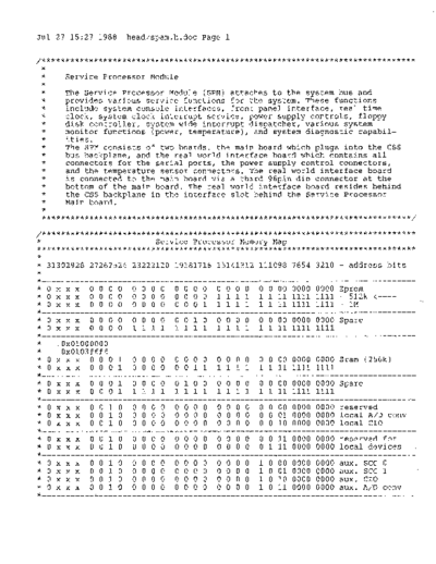
Jul 27 15:27 1988 head/spam.h.doc Page 1
/*******************************************************************************
*
* Service Processor Module
*
* The Service Processor Module (SPM) attaches to the system bus and
* provides various service functions for the system. These functions
* include system console interfaces, front panel interface, real time
* clock, system clock interrupt service, power supply controls, floppy
* disk controller, system wide interrupt dispatcher, various system
* monitor functions (power, temperature), and system diagnostic capabil-
* ities.
* The SPM consists of two boards, the main board which plugs into the ess
* bus backplane, and the real world interface board which contains all
* connectors for the serial ports, the power supply control connectors,
* and the temperature sensor connectors. The real world interface board
* is connected to the main board via a third 96pin din connector at the
* bottom of the main board. The real world interface board resides behind
* the ess backplane in the interface slot behind the Service Processor
* Main board.
*
******************************************************************************/
/*******************************************************************************
* Service Processor Memory Map
********************************************************************************
*
* 31302928 27262524 23222120 19181716 15141312 111098 7654 3210 - address bits
*
*-------------------------------------------------------------------------------
* 0 x x x o 0 0 0 o 0 0 0 o 0 0 0 a 0 0 0 a a 00 0000 0000 Eprom
* 0 x x x o 0 0 0 o 0 0 0 o 0 0 0 1 1 1 1 1 1 11 1111 1111 - 512k <----
* 0 x x x o 0 0 0 o 0 0 0 o 0 0 1 111 1 1 1 11 1111 1111 - 1M
*-------------------------------------------------------------------------------
* a x x x 0 a 0 0 0 0 0 0 0 0 1 0 0 a a a 0 0 00 0000 0000 Spare
* 0 x x x 0 0 0 0 1 1 1 1 1 1 1 1 1 1 1 1 1 1 11 1111 1111
*-------------------------------------------------------------------------------
* Ox01000000
* Ox0103ffff
* o 000 000 0 a a 0 0 o 0 00 0000 0000 Sram (256k)
0 x x x 0 0 0 1
* o 0 0 0 a a 1 1 1 1 1 1 1 1 11 1111 1111
0 x x x 0 0 0 1
*-------------------------------------------------------------------------------
* 0 x x x a 0 0 1 o 0 0 0 o 1 0 0 000 0 o 0 00 0000 0000 Spare
* 0 x x x o 0 0 1 1 1 1 1 111 1 111 1 1 1 11 1111 1111
*-------------------------------------------------------------------------------
* 0 x x x 0 0 1 0 a a 0 0 0 0 a 0 0 0 a 0 0 0 00 0000 0000 reserved
* 0 x x x 0 a 1 0 0 0 0 0 a 0 0 0 a 0 0 0 0 0 01 0000 0000 local A/D conv
* 0 x x x 0 0 1 0 0 a 0 a 0 a 0 0 0 a 0 a 0 0 10 0000 0000 local eIa
*-------------------------------------------------------------------------------
* 0 x x x a 0 1 0 a 0 a 0 0 0 0 0 0 0 0 a a 0 11 0000 0000 reserved for
* 0 x x x 0 0 1 0 0 0 0 0 0 0 0 0 0 0 0 0 0 1 11 0000 0000 local devices
*-------------------------------------------------------------------------------
* 0 x x x 0 0 1 0 0 0 0 0 0 0 0 0 0 0 0 0 1 0 00 0000 0000 aux. see 0
* 0 x x x a 0 1 0 0 0 0 0 0 0 0 a 0 0 0 0 1 0 01 0000 0000 aux. see 1
* 0 x x x 0 0 1 0 0 0 0 0 0 0 0 0 0 0 0 0 1 0 10 0000 0000 aux. eIa
* 0 x x x 0 0 1 0 0 0 0 0 0 0 0 0 0 0 0 0 1 0 11 0000 0000 aux. A/D conv
*-------------------------------------------------------------------------------
Jul 27 15:27 1988 head/spam.h.doc page 2
* 0 x x x 0 0 1 0 0 0 0 0 0 0 0 0 0 0 0 0 1 1 11 0000 0000 aux. devices
0 0 0 0 0 0 0 0 0 0 0 00 reserved for
* 0 x x x 0 0 1 0 0 1 1 0000 0000
*-------------------------------------------------------------------------------
* 0 x x x 0 0 1 1 1 1 1 1 1 1 1 1 1 1 1 1 1 1 11 1111 1111 and NV ram clock
x 0 0 0 0 0 0 0 0 0 0 0 0 0 0 00 0000 0000 real time
*0 x x 0 0 1 1
*-------------------------------------------------------------------------------
* 0 x x x 0 1 0 0 1 1 1 1 1 1 1 1 1 1 1 1 1 1 11 1111 1111 reserved
x 0 0 0 0 0 0 0 0 0 0 0 0 0 0 00 0000 0000
* 0 x x 0 1 0 0
*-------------------------------------------------------------------------------
* 0 x x x 0 1 0 1 0 0 0 0 0 0 0 0 0 0 0 0 0 0 00 0000 0000 clock control
*-------------------------------------------------------------------------------
* 0 x x x 0 1 0 1 1 1 1 1 1 1 1 1 1 1 1 1 1 1 11 1111 1111 reserved
x x 0 0 0 0 0 0 0 0 0 0 0 0 0 0 00 0000 0001
*0 x 0 1 0 1
*-------------------------------------------------------------------------------
* 0 x x x 0 1 1 0 1 1 1 1 1 1 1 1 1 1 1 1 1 1 11 1111 1111 reserved
0
x x x
0 1 1 0
0 0 0 0 0 0 0 0 0 0 0 0 0 0 00 0000 0000
*
*-------------------------------------------------------------------------------
* 0 x x x 0 1 1 1 0 0 0 0 0 0 0 0 0 0 0 0 0 0 00 0000 0000 Wr cntl 0 (read)
* 0 x x x 0 1 1 1 0 0 0 0 0 0 0 0 0 0 0 0 0 0 00 0000 0000 Wr cntl 1
x 0000 cntl 0
* 0 x x x 0 1 1 1 0 0 0 0 0 0 0 0 0 0 0 0 0 0 00 0010 0000 Wr cntl 1 (read)
0 x x 0 1 1 1 0 0 0 0 0 0 0 0 0 0 0 0 0 0 00 0010 Wr
* 0 x x x 0 1 1 1 0 0 0 0 0 0 0 0 0 0 0 0 0 0 00 0100 0000 Wr cntl 2
* 0 x x x 0 1 1 1 0 0 0 0 0 0 0 0 0 0 0 0 0 0 00 0100 0000 Wr cntl 2 (read)
* 0 x x x 0 1 1 1 0 0 0 0 0 0 0 0 0 0 0 0 0 0 00 0110 0000 Reserved
*
* 0 x x x 0 1 1 1 0 0 0 0 0 0 0 0 0 0 0 0 0 0 00 1010 0000 CSS command reg
1 1 0 0 0 00 1000
* 0 x x x 0 1 1 1 0 0 0 0 0 0 0 0 0 0 0 0 0 0 00 1100 0000 CSS error reg
x 0 0 0 status reg
* 0 x x x 0 1 1 1 0 0 0 0 0 0 0 0 0 0 0 0 0 0 00 1110 0000 Dispatcher error
x 0 0 0
*0 x 0 1 0 0 0 0 0 0000
register
*
*-------------------------------------------------------------------------------
* 0 x x x 0 1 1 1 1 1 1 1 1 1 1 1 1 1 1 1 1 1 11 1110 1111 Spare
0 0 0 0 0 0 0 0 0 0 0 0 0 0 00 0001
*0 x x x 0 1 1 1 1111
*-------------------------------------------------------------------------------
0 0 0 0 1 0 0 0 0 0 0 0 0 0 0 0 0 0 0 0 0 0 00 0000 0000 Map RAM loc 0
* 1
* 0 0 0 1 1 0 0 0 0 0 0 0 0 0 0 0 0 0 0 0 0 0 00 0000 0000 " " "
* 0 0 1 0 1 0 0 0 0 0 0 0 0 0 0 0 " 0 0 02 0 0 0 00 0000 0000 " "
* 0 0 1 1 1 0 0 0 0 0 0 0 0 0 0 0 " 0 0 " 3
0 0 0 0 00 0000 0000 "
* 0 1 0 0 1 0 0 0 0 0 0 0 0 0 0 0 " 0 0 " 4
0 0 0 0 00 0000 0000 "
* 0 1 0 1 1 0 0 0 0 0 0 0 0 0 0 0 " 0 0 " 5
0 0 0 0 00 0000 0000 "
* 0 1 1 0 1 0 0 0 0 0 0 0 0 0 0 0 " 0 " 0 " 6
0 0 0 0 00 0000 0000
* 0 1 1 1 1 0 0 0 0 0 0 0 0 0 0 0 " 0 " 0 " 7
0 0 0 0 00 0000 0000
*-------------------------------------------------------------------------------
* 0 x x x 1 0 0 1 1 1 1 1 1 1 1 1 1 1 1 1 1 1 11 1111 1111 Floppy Disk
0 x x
x
1 0 0 0
0 0 0 0 0 0 0 0 0 0 0 0 0 0 00 0000 0000
*
*-------------------------------------------------------------------------------
* 0 x x x 1 0 1 0 1 1 1 1 1 1 1 1 1 1 1 1 1 1 11 1111 1111 reserved
x x x 1 0 0 0 0 0 0 0 0 0 0 0 0 0 0 00 0000 0000
* 0 1 0 0
*-------------------------------------------------------------------------------
* 0 x x x 1 a 1 1 a a 0 0 0 0 0 a a a a a a 0 00 0000 1111 LD. Idle Queue
x 0 0 0 0 0 0 a a 0
a 0 0 0 0 00 0000
0000
*0 x x 1 1 1 0
*-------------------------------------------------------------------------------
* a x x x 1 0 1 1 1 1 1 1 1 1 1 1 1 1 1 1 1 1 11 1111 1111 unused
a a a 0 0 0 0 0 0 a 0 0 0 0 00 0001 0000
* 0 x x x 1 0 1 1
*-------------------------------------------------------------------------------
* 0 x x x 1 1 a 0 0 a 0 a a a 0 a a 0 1 1 1 1 11 1111 1111 LD. Queue Ram
x x 0 0 0 0 0 0 0 0 0 0 0 0 0 0 00 0000 0000
*0 x 1 1 0 0
Jul 27 15:27 1988 head/spam.h.doc Page 3
*-------------------------------------------------------------------------------
* 0 x x x 1 1 0 0 0 0 0 0 0 0 0 0 0 1 0 0 0 0 00 0000 0000 unused
* 0 x x x 1 1 0 0 1 1 1 1 1 1 1 1 1 1 1 1 1 1 11 1111 1111
*-------------------------------------------------------------------------------
* 0 x x x 1 1 0 1 0 0 0 0 0 0 0 0 0 0 0 0 0 0 00 0000 0000 I.D. Pointer Ram
* 0 x x x 1 1 0 1 1 1 1 1 1 1 1 1 1 1 1 1 1 1 11 1111 1111
*-------------------------------------------------------------------------------
* 0 x x x 1 1 1 0 0 0 0 0 0 0 0 0 0 0 0 0 0 0 00 0000 0000 Int Dispatcher
* 0 x x x 1 1 1 0 1 1 1 1 1 1 1 1 1 1 1 1 1 1 11 1111 1111 Misc. Rams
*-------------------------------------------------------------------------------
* 0 x x x 1 1 1 1 0 0 0 0 0 0 0 0 0 0 0 0 0 0 00 0000 0000 reserved
* 0 x x x 1 1 1 1 1 1 1 1 1 1 1 1 1 1 1 1 1 1 11 1111 1111
*-------------------------------------------------------------------------------
/******************************************************************************
*
* EPROM
*
* The EPROM is 8 bits wide and can be read by the processor on data bits
* 24 to 31. There are 2 sockets for the EPROM, one or both can be populat-
* ed with either 27256s (32k x 8 each), or 27512s (64k x 8 each) or
* 271001s (128k x 8 each). Address bits Add.OO to Add.15 or Add.16 or
* Add.17 are used to address the EPROM. The decoding of the high bit is
* controlled by the Promsize field in control register 2. This allows the
* two EPROM chips to be contiguous regardless of their size. (See Control
* register 2 description for details).
*
******************************************************************************/
#define PROMSIZ Ox10000 /* cpu monitor prom*/
#define PROMSTART OxOOOOOOOO /* start of prom area */
/*******************************************************************************
*
* Static Ram
*
* The SRAM is 32 bits wide and consists of 8 or 4 32k x 8 static RAM chips
* for 64k x 32 or 32k x 32 bits of memory. It is addressed with address
* bits Add.02 to Add.17.
*
******************************************************************************/
#define SRAMSTART Ox01000000
#define SRAMSIZE Ox40000
/*******************************************************************************
*
* Real Time Clock
*
* The real time clock is a MK48T12 chip. This chip has a built in crystal
* oscillator and a lithium battery. In addition to a real time clock, it
* has 2K bytes of nonvolatile RAM. This RAM can be used to keep config-
* uration information. The service processor does not have any switches.
*
******************************************************************************/
#define RTC ((struct rtc *)(Ox030007f8))
Jul 27 15:27 1988 head/spam.h.doc Page 4
/*******************************************************************************
*
* Local A/D converter
*
* The local A/D converter is an Mc14442 and a TL431A voltage reference.
* It is used to measure the temperature on the Service Processor (i.e. the
* cardcage) and the 6 voltages present on the SPM(i.e. +SV main, +SV aux.,
* +12V main, +12V aux., -12V main, and -12V aux.)
*
******************************************************************************/
#:define ADC CNTL ((unsigned short*)(Ox02000102))
#:define ADC-ADATA ((unsigned short*)(Ox02000100))
#:define ADC-SC Ox01OO
#:define ADC-CHO OxOOOO /* measures +5v for master system */
#:define ADC-CHl OxOOOl /* reference voltage 4.5v must read FF */
#:define ADC-CH2 OxOOO2 /* Measure +Sv. aux */
#:define ADC-CH3 OxOOO3 /* Measure +12v */
#:define ADC-CH4 OxOOO4 /* Measure +12v aux */
#:define ADC-CH5 OxOOO5 /* Measure -12v */
#:define ADC-CH6 OxOOOe /* Measure -12v aux */
#:define ADC-CH7 OxOOOf /* measure on board temperature. */
#:define ADC-EOC Ox8000
#:define ADC-MASK OxOOff /* mask for valid data. */
/*******************************************************************************
*
* Local CIO
*
* The local CIO is a Zilog 8036, used for various timing functions includ-
* ing the CSS bus timeout and the main system clock interrupt.
*
******************************************************************************/
#:define LOCCIO ((struct cio *)(Ox02000200))
/*******************************************************************************
*
* SCC
*
******************************************************************************/
#:define ASCC ((struct ascc *)(Ox02000800))
#define AUXASCCOB ((struct ascc *)(Ox02000800))
#:define AUXASCCOA ((struct ascc *)(Ox02000820))
#:define AUXASCCIB ((struct ascc *)(Ox02000900))
#:define AUXASCCIA ((struct ascc *)(Ox02000920))
/*******************************************************************************
*
* Clock Control (write only)
*
* The Clock control port is a single bit port which is written with data
* bit O. Data.OO = 0 means the CPU is using its on-board lOMhz clock,
* Data.OO = 1 means the CPU is using the CSS bus clock divided by two as
* its clock source. When switching from one clock source to the other,
Jul 27 15:27 1988 head/spam.h.doc Page 5
* approximately 1us after the write to the clock control port, the hard-
* ware will issue a reset to the CPU, hold the reset for approximately
* 500us, and switch clocks during the reset. This is required to meet the
* timing specifications of the 68020. In the process, the entire board
* will be reset, so any VLSI chips will have to be reinitialized. The
* memory, however, will keep its data valid. The state of the clock bit
* (i.e. which clock is being used) can be read in the status register. If
* the CSS bus clock is not running(e.g. the CSS bus is powered down), the
* hardware will not select the CSS clock.
*
* 31 ---------- 1 0
* +---------------+-+
* I x Icl
* +---------------+-+
* I I
* I +--------------
0 - on board 10Mhz clock
* I 1 - CSS bus clock
* +----------------------- unused
******************************************************************************/
#define CLKCNTL ((unsigned *)(Ox05000000))
/*******************************************************************************
*
* CSS Command Register (read only)
*
* The CSS command register is a 32 bit register which allows the local CPU
* to read the value written to the SPM via a CSS write to addr OxXXXXAAYY
* by any other CSS module. X's are don't cares and AA will be captured by
* the SPM and can be read in the Status register. YY must be of the form
* OOOX XXXX. The SPM only decodes the top three bits of the least signif-
* icant byte of CSS address. When another module writes to an address of
* the form described above on the SPM, the 68020 recieves an interrupt
* informing it that a CSS command has been received. The 68020 will read
* the CSS command register and the status register to determine the data
* of the command.
*
* 31 ---------- 0
* +---------------+
* I command I
* +---------------+
* I
* +----------------------- command to SPM via CSS write
*
******************************************************************************/
#define CSSCMD ((unsigned *)(Ox07000080))
/*******************************************************************************
*
* Status Register (read only)
*
* The status register is a 24 bit register, data bits 00 to 07 and 16 to
* 23 and 24 to 31 can be read by the 68020. Bits 24 to 27 are the bus slot
* number given by the position of the SPM in the backplane. For diagnostic
Jul 27 15:27 1988 head/spam.h.doc Page 6
* purposes, the 5PM does not have its slot id hardwired, so for the board
* to function properly, the slot id must be read in the status register
* and written in write control registers 0 and 1. Bit 31 in the 5tatus
* register is a status bit from the interrupt dispatcher state machine.
* When this bit is 0, the interrupt dispatcher has suspended its dispatch-
* ing function and the CPU is allowed to access the various RAMs in the
* interrupt dispatcher. This is needed for initializing the interrupt
* dispatcher and for diagnostic purposes. When the bit is a 1, the
* interrupt dispatcher is in its normal operating mode and the CPU must
* not access any of the dispatcher RAMs. Bit 30 is an indicator from the
* floppy disk, floppy ready. Bit 29 is a status bit from the clock select
* mechanism. When this bit is a 1, the 68020 is using the local clock,
* when 0, the 68020 is using the C55 clock divided by 2. Bit 28 is reserv-
* ed. Bits 00 to 07 are part of the C55 error register as follows:
* Bit 00 has the state of the C55 bus nack signal at the time of the last
* C55 bus error, bit 01 has the state of the C55 bus ack, bit 02 has the
* state of the C55 arbiter grant error, bit 03 is the bad command bit.
* This bit is a 0 if the 5PM has detected a C55 bus protocol violation
* (e.g. data parity is bad), it is a 1 if the 5PM has not detected such
* a violation but it has nevertheless detected a C55 bus error. Bit 04
* is the state of the C55 arbiter burst signal. Bits 05 to 07 are reserv-
* ed. Bits 16 to 23 are the C5S data byte 6 at the time of the most recent
* C55 command write.
*
* 31 30 29 28 27 - 24 23 - 16
* +--+----+--+--+-------+-------+
* IIDIFRDYI cl xlslot # 1 byte 61
* +--+----+--+--+-------+-------+
* 1 1 1 1 1 1
* 1 1 1 1 1 +----- C55 data byte 6 at the time of the mo~
* 1 1 I I I recent C55 command write.
* 1 I I I +------------- bus slot # determined by position of
* I I I I 5PM in backplane
* I I I +------------------ reserved
* I I +---------------------
1 = local clock
o = CSS clock
* I I
* I +------------------------- floppy ready
* +------------------------------ from Interrupt Dispatcher state machine
o - dispatcher has been suspended and
* the cpu is allowed access to ID rams
* 1 - Int Dispatcher normal mode, cpu
* should not access dispatcher RAM's
*
* 15-8 7-6 5 4 3 2 1 o
*
* +----+---+--------+------+-------+-----+----+----+
* I x I I active Iburst*lbad cmdlgerr*lbacklnackl
* +----+---+--------+------+-------+-----+----+----+
* I I I I I I I I
* I I I I I I I +-state of C55 bus nack
* I I I I I I I signal at the last
* I I I I I I I C5 5 bu s err 0 r
* I I I I I I +-- state of C55 bus ack
* I I I I I +--------- state of CSS arbi ter
* I I I I I gran t err 0 r
* I I I I +---------------- bad command bi t
* I I I I 0 - SPM has detected a CSS bu,ii
Jul 27 15:27 1988 head/spam.h.doc Page 7
* protocol violation(data
* parity is bad)
* 1 - SPM has not detected a
* violation, but detected a
* ess bus error
* +----------------------- state of ess arbiter
* burst signal
*
*
+------------------------------- always ack,nack,grant errors
force
a 1 except during
* +------------------------------------- reserved
* +------------------------------------------ unused
*
******************************************************************************/
*define STATUSREG ((unsigned *)(Ox070000aO))
*define STAT SLOTMASK OxOfOOOOOO
*define STAT-SLOTSH 24
*define STAT-REG IDRAM Ox80000000
*define STAT-IDLE FULL OxlOOOOOOO /* if set, idle-que is not full. */
/*******************************************************************************
*
* ess Error Register (read only)
*
* When the SPM detects an error on the ess bus the hardware will interrupt
* the 68020. The 68020 will read the ess error information register to
* determine the nature of the error. The conditions which cause such an
* error are: bad data parity, bad type parity, destination error, source
* error, invalid type, bus nack, or grant error. All error conditions
* except the last two will latch in valid data for the ess error informa-
* tion register as shown below. Additional error information is captured
* in the status register. When a bus error condition has been latched in
* the error register no new error conditions can be latched until after
* the bus error register has been read by the 68020.
* 31 - 27 26-25 24 23-20 19-16 15 14 13-8 7-0
* +--------+-----+----+-----+-----+----+----~+--.,..-+,----+
*
* less datal x Ibparldest I src Iderrlserrlbtypelbparl
* +--------+-----+----+-----+-----+----+-----+----+----+
* I I I I I I I I I
* I I I I I I I I +- bus data pari ty
* I I I I I I I I 0 - 7
* I I I I I I I +------ bus type 0 - 5
* I I I I I I +----------- source error
* I I I I I +---------------- destination error
* I I I I +---------------------- bus source 0 to 3
* I I I +---------------------------- bus dest 0 to 3
* I I +--------------------------------- bus type parity
* I +--------------------------------------- reserved
* +----------------------------------------------- ess data bits 57,40-43
*
******************************************************************************/
*define eSSERROR ((unsigned *)(Ox070000cO))
*define DERR 15
*define SERR 14
Jul 27 15:27 1988 head/spam.h.doc Page 8
#define BTYPE SH 8
:ft:define SRC sa 16
#define DEST SH 20
:ft:define BPAR-SH 24
:ft:define BPAR-MASK Ox01000000
:ft:define DEST-MASK OxOOfOOOOO
:ft:define SRC MASK OxOOOfOOOO
:ft:define BTYPE MASK Ox00003fOO
:ft:define TYPE SH OxOb
#define TYPE-MASK Ox3800
:ft:define SIZE-MASK Ox0700
:ft:define SIZE-SH Ox08
/*******************************************************************************
* Dispatcher Error Register
*
* When the Interrupt Dispatcher detects an error it will suspend its
* operation and latch error information in this register.
* 31 - 24 23 22-20 19-18 17-16 15-12 11-8 7 6-0
*
* +--------+----+-----+-----+-----+-----+-----+---+---+
* lInt Vecldintl err I x I pri Idest I src lintlsrcl
* +--------+----+-----+-----+-----+-----+-----+---+---+
* I I I I I I I I
* I I I I I I I +-- i/o bus source slot
* I I I I I I I (only valid if bit 7=1)
* I I I I I I +------- i/o bus int
* I
I .I I I I I 1 - int came from an
i/o module
*
* I I I I I I 0 - int came from a CSS
* I I I I I I bus module
* I I I I I +------------ CSS bus source slot
* I I I I +----------------- CSS bus dest slot
* I I I +----------------------- Interrupt priority
* I I +----------------------------- reserved
* I
I
+---------------------------------- error code
(see below for codes)
*
* +---------------------------------------- Directed interrupt
* +------------------------------------------------ Int vector number
*
* error information bits 22 21 20
*
* x x o - request error
* 1 0 x - ack error, bus error on ack response
* o 0 x - ack error, no previous requests
* x 1 1 - recieve error, fix pointers or reset
* recieve
*
*
******************************************************************************/
:ft:define DISPERROR ( (unsigned *)(Ox070000eO))
#define DISP ACK ERR 1 /* insane ack, an ack for no good reason */
:ft:define DISP-REQ-ERR 2 /* request with no into pending */
/* unused - 3 /* recieve err */
/* unused 4 /* */
Jul 27 15:27 1988 head/spam.h.doc Page 9
ide fine DISP ACK TOUT 5 /* timeout on ack response */
ide fine DISP-REQ-TOUT 6 /* timeout on request */
idefine DISP-RCV-ERR 7
#define DISP-ERR-SH 20
/*******************************************************************************
* write Control Register 0 (write only)
*
* 31-29 28 27 26 25 24 23-20 19-16
* +-----+-----+-----+------+-----+-----+------+-----+
*
* I linh7 Ifreezl dest Igrantl ack IsrcID*lsrcIDI
* +-----+-----+-----+------+-----+-----+------+-----+
* I I I I I I I
* I I I I I I +--- -- out.src 0-3 source id
* I I I I I I used by SPM when it is
* I I I I I I issuing a command
* I I I I +-------- out. src 0 to 3*
* I I I I omplement of source id
* I I I +-----------------'-'- force ack/nak er ror.
* I I I
* I I +------------------------- force grant error.
* I I
* I +------------------------------- force bad dest.
* I
* +------------------------------------- Freeze CPU bit:
active 1 (Must have
* CSS Reset rdy 1)
*
* +------------------------------------------- Inhibit level 7
CSS int's.
*
*
* +-------------------------------------------
*
*
* 15-12 11-8 7-6 5-0
* +------+------+---+-----+;~-
* 'C)
* IslotIDIslotIDlf10lFtypei
* +------+------+---+-----+
*
* I I I~- forced type
* I I I,!~. (used if "use. forced. type" bit is active)
* I I +----~-- forced address bits 00 & 01
* I +----------~--- slot id used by int dispatcher
* I (tells SPM where to place pointers for
* I non-dir ints 0-3)
* +--------------------- slot pretend to be CSS backplane
(to
id used with
a CPU)
*
*
******************************************************************************/
idefine WRCNTLO ((unsigned *)(Ox07000000))
idefine WRO FTYPE MASK Ox0000003f
idefine WRO-FADDOT MASK OxOOOOOOcO
idefine WRO-FADD01-SH Ox06
idefine WRO-PRETEND MASK OxOOOOfOOO
Jul 27 15:27 1988 head/spam.h.doc Page 10
#define WRO PRETEND SH 12
#define WRO FRC ACK- Ox01000000
#define WRO-FRC-GRANT Ox02000000
#define WRO-FRC-DEST Ox04000000
#define WRO-FRC-FREE Ox08000000
#define WRO-FRC-INH7 Ox10000000
/*******************************************************************************
* Write Control Register 1 (write only)
*
* 31 30 29 28 27 26 25 24
*
* +---+---+----+----+-----+----+----+----+
* lacklrdylrrdylfmodlfdestldiagldiagldreql
* +---+---+----+----+-----+----+----+----+
* I I I .'. .
.,.Iu::.,., cpu.disp.req*
* I I I :l~
* I I I 11" ' , o - indicates to int dispatcher that
* I I I 68020 wants to access its rams.
* I I I 1 - int dispatcher resumes normally.
* I I +--- diag.frc.int.rec*
* I I o - decode a CSS cpu int request
* I I level as a CSS command.
1 - normal mode.
+--------1~
* I I
* I '. diag.any.type*
* I o - accept any CSS bus action as a
* I valid response to a SPM
.'
* I initiated read request.
* I . wi. 1 - normal mode.
* +--------------:1&.- use.fake.dest*
* o - destination at arbiter is forced
* to be bits 8 to 11 of cntl reg 1
* 1 - normal - dest at arbiter is the
* same as the dest which will be
* used on the CSS bus with the
* requested CSS bus transaction.
* +----------------------- force.modify*
* o - forces a modify cycle on the CSS
* bus as long as the bit is 0
* +__________________________ -L:.~p~.~~~~~!a~~~e.
* V r'-1:~◦ Jabse Service Manual Search 2026 ◦ Jabse Pravopis ◦ onTap.bg ◦ Other service manual resources online : Fixya ◦ eServiceinfo