Service Manuals, User Guides, Schematic Diagrams or docs for : . Various Car Audio chrysler
<< Back | HomeMost service manuals and schematics are PDF files, so You will need Adobre Acrobat Reader to view : Acrobat Download Some of the files are DjVu format. Readers and resources available here : DjVu Resources
For the compressed files, most common are zip and rar. Please, extract files with Your favorite compression software ( WinZip, WinRAR ... ) before viewing. If a document has multiple parts, You should download all, before extracting.
Good luck. Repair on Your own risk. Make sure You know what You are doing.
Image preview - the first page of the document
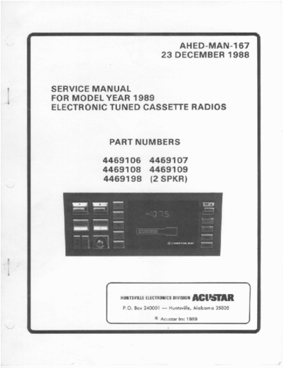
>> Download chrysler documenatation <<
Text preview - extract from the document
4. Voltaae Tuned AM Circuits - The capacitances of
varactors Dl, D2, and D3, in 'the AM tuner module
U2, change when the DC voltage applied across them
changes and the resonant frequencies of their
associated L-C circuits are changed. When a
varactor fails, replace the U2 module.
5. Voltaue Tuned FM Circuits - The capacitances of the
FM varactors, located in module lJ4, change when the
DC voltage applied across them changes and the
resonant frequencies of their associated L-C
circuits are changed. When a varactor fails,
replace the U4 module.
E. CLEANING
Because of the inaccessibility of the Tape Mechanism, a
combination head and capstan cleaning tape should be used. If
the radio is disassembled, the heads, pinch rollers and capstan
shafts may be cleaned with isopropyl (rubbing) alcohol.
III. CIRCUIT DESCRIPTION
A. LOGIC AND CONTROL CIRCUITS
The logic and control functions of the receiver are performed
primarily on the Audio/Logic PC Board, by the microprocessor
UlOO (see Table l-3), and the frequency synthesizer U102. The
microprocessor accepts commands from the pushbutton switches
located on the front of the radio and status signals from the
RF board, cassette module and compact disc (CD) player
(INFINITY ONLY). It processes the information and generates
instructions to the display module and the frequency
synthesizer. The display driver controls the vacuum
fluorescent display and is located in the VF display module on
the control PC board. The frequency synthesizer controls the
local oscillator frequency and, thereby, the tuning of the
radio. The synthesizer will tune either 200 kHz/lO kHz for
U.S. use or 100 kHz/9 kHz steps for European use. European or
U.S. mode selection is accomplished by software. To change the
operating mode, press the SET key then the SEL key and press
the memory one button three times in succession. For a
description of synthesizer pin functions, see Table l-4.
1-13
TABLE 1-3. MICROPROCESSOR (UlOO) PIN DESCRIPTIONS
PIN NUMBER DESCRIPTION
1 Key Input KO
2 Key Input Kl
3 Key Input K2
4 Key Input K3
5 Radio Test Pin
6 Frequency Synthesizer Enable - Allows data
transfer to the Frequency Synthesizer
7 Beep Output
8 Soft mute goes low to turn on Q102
9 Reset Input - A high on this pin for 6
usec. while the oscillator is running
resets the device.
10 Serial data input and output - Provides
serial data to the display driver and
frequency synthesizer.
11 Serial Clock - The serial data clock.
12 Tape Reel Input - Internally pulled up.
13 Off/On Key Input
14 CD "On" Input - Goes low for CD in.
15 I2 C Data
16 I2 C Clock
17 Power antenna on
18 N/C
19 External Oscillator - 1.98 MHz fed from
the synthesizer
20 Ground
21 Used for display blanking
l-14
TABLE 1-3. MICROPROCESSOR (UlOO) PIN DESCRIPTIONS (Cont.)
PIN NUMBER DESCRIPTION
22 Cassette read enable
23 Cassette write enable
24 AM Mono - Goes low for force to mono
25 Station detect - goes low for station
26 Joystick enable
27 Stereo Detect - goes low for stereo
28 Display Driver Enable - Allows data to be
transferred to the vacuum fluorescent
display driver.
29 N/C
30 W C
31 External access connected to Vcc
32 Goes low for hard mute output to turn on
QlOl
33 Power Switch Input - Goes high for
ignition on
34 Goes high for FM
35 Goes high for AM
36 Strobe 3
37 Strobe 2
38 Strobe 1
39 Strobe 0
40 Voltage Supply, Vcc + 5VDC
l-15
TABLE l-4. SYNTHESIZER (U102) PIN DESCRIPTIONS
PIN NUMBER DESCRIPTION
1 Goes high during the search mode, to
desensitize the front end to very weak
stations.
2 Noise Reduction (high = NR on)
3 Serial data from the microprocessor
4 Data clock from the microprocessor
5 Data enable from the microprocessor
6 Switched supply voltage which is
regulated by U103, a 5 volt regulator.
7 Input from the AM local oscillator
8 External bypass capacitor for the phase
detector
9 Input from the FM local oscillator
10 Ground
11 Unswitched supply voltage (Vcc) for
the clock keep alive. Keeps the
synthesizer oscillator and dividing chain
active when the remaining functions of the
synthesizer are powered down. Provides a
low power microprocessor clock driver and
a time-of-day indication.
12, 13 Reference oscillator which is controlled
for stability by a quartz crystal (X101),
capacitors and trimmer capacitor, for
accurate setting of the clock.
14 Reference oscillator frequency divided by
two from which the microprocessor derives
the instruction time.
15 Clock signal (50 Hz) used in the program
loop timing.
16 Resistor R124 sets the gain of the phase
locked loop.
1-16
TABLE l-4. SYNTHESIZER (U102) PIN DESCRIPTIONS (CONT.)
PIN NUMBER DESCRIPTION
17 Charge pump output develops tuning
voltages and op-amp input.
18 Operational amplifier output - Supplies
the tuning voltage for the RF circuits.
19 Operational amplifier ground.
20 Switched supply voltage, 10 volts.
1. Power-On-Reset - The power-on-reset is controlled
by UlOl, see Table l-5. Input pin 2 is always high
except when the battery voltage is disconnected.
When the ignition voltage is applied, the RC time
constant of Cl16 and R107 causes a pulse to be
applied to pins 8 and 9, which causes pin 10 to go
to a logic low. Pin 10 is hard wired to pin 1.
With a logic high on pin 2 and a logic low on pin
1, the output pin 3 goes high. When pin 3 goes
high, the microprocessor resets and pins 8 and 32
of the microprocessor go high. This turns on QlOl
and QlO2, which causes the mute pin 11 of the audio
output IC'S to go low, therefore, muting the
output.
TABLE 1-5. QUAD 2 INPUT NAND SCHMITT-TRIGGER
INPUT A INPUT B OUTPUT
2. Analog to Digital Converter - The joystick provides
a balance and fader input to A/D converter U202
which places information on the Bus to allow the
microcomputer to control U105 for these functions.
1-17
B. AM CIRCUIT
1. RF Stage - The AM signals received by the antenna
are coupled through the series choke Ll, which
presents a high impedance to FM and shortwave
broadcast frequencies, and Cl to AM antenna coil Tl
which transformer couples the RF signal to the gate
of Ql a J-FET RF amplifier. Transistor Q2 the
second RF amplifier has its conduction controlled
by the RF amplifier AGC pin 1 of Ul. The RF output
of Q2 is applied to pin 1 of U2 which contains a
varactor diode, fixed capacitor, trimmer capacitor
and transformer tuned to resonate at the selected
frequency.
2. Local Oscillator - The local oscillator tuning is
accomplished through pin 20 of Ul. The local
oscillator is controlled by the synthesizer and
tuned by the combination of fixed capacitors,
trimmer capacitor, transformer and a varactor diode
in U2. The output of the oscillator goes directly
to the mixer and also the synthesizer.
3. Mixer Staae - The mixer input is tuned by a
varactor diode, fixed capacitor, trimmer capacitor
and transformer contained in U2. The RF and
oscillator are heterodyned in the mixer. The mixer
output pin 7 of Ui is tuned to resonate at the IF
or difference frequency by FL1 and applied to the
IF input pin 9 of Ul through C8.
4. IF S t a g e - Pin 9 of Ul is the IF input which is
amplified internally in Ul, and outputted on pin 10
of Ul. The stage gain of the IF amplifier is
controlled by the IF AGC pin 17 of Ul. The IF out
is tuned by T2 and coupled by Cl7 to the base of
Q3. Transistor Q3 and Q4 are in the cascade
configuration with the output being taken off the
collector of Q4 and applied to the AM stereo
decoder U3.
5. AM Station Detect - When an AM signal is received,
the signal meter or station detect output pin 16 of
Ul will cause Q7 to conduct which will result in
Jl-11 going low. When an AM station is not
received, Q7 will be cut off and Jl-11 will go
high.
6. Detector and AM Stereo Decoder - The AM stereo
decoder chip, U3, contains circuitry to detect and
decode AM stereo from stations using the Motorola
C-Quam AM stereo system. This system uses a
modified form of quadrature modulation which is
l-18
6. Detector and AM Stereo Decoder (Cont.)
compatible with monaural receivers. The phase
modulation components of a quadrature signal are
extracted and used to phasemodulate the broadcast
transmitter. The (L-R) information is contained in
this quadrature phase modulation. The (L+R) is
transmitted as normal AM. The chip automatically
switches to decode stereo when a 25 Hz, 4%
modulated pilot signal is received. Stations
transmitting other systems of AM stereo are
received in monaural, as are non-stereo stations.
The 450 kHz AM intermediate frequency is applied to
pin 3 of u3. The chip contains an envelope
detector which detects the (L+R) portion of the
signal. A phase locked loop (PLL) detector,
utilizing an external resonator controlled
oscillator, which operates at eight times the IF
frequency, to detect the (L-R) portion of the
signal. The frequency of the oscillator is 3600
kHz and is applied to pin 17 with pin 18 being the
feedback pin.
The stereo pilot signal is contained in the phase
modulated (L-R) portion of the signal. This signal
is controlled by an internal AGC and outputted on
pin 11. A low pass filter is formed by R19 and
C20, from which point the signal goes to pin 13,
the input of a 25 Hz bandpass filter. The output
of the bandpass filter appears at pin 14, which is
also the pilot detector input. The pilot detector
has two modes of operation. With a good signal it
will switch to stereo after seven consecutive
cycles of the 25 Hz pilot. When interference is
present the pilot detector requires 37 consecutive
cycles of pilot to switch to stereo. Pin 12 of U3
is the interference detector input. If the
detected low frequency phase modulated interference
exceeds a certain level, the pilot detector will be
prevented from switching to stereo. A greater
level of interference is required to switch back to
monaural if the pilot detector is already in
stereo. The most common type of interference that
would require the circuitry to switch to monaural
mode, would be the reception of more than one
station on the selected frequency. Pin 15 goes low
to indicate stereo. The decoder can be forced to
monaural by holding pin 9 low. When any tuning
function is operated, pin 9 is hold low by the
microprocessor to switch the decoder to monaural
for approximately 1 second.
l-19
6. Detector and AM Stereo Decoder (Cont.)
During AM operation, transistors Q5 and Q6 conduct
to apply the regulated 10 volts to pin 6 of U3.
The AM audio outputs pin 7 (left) and pin 8 (right)
are applied to the filter/Amp IC (U7).
C. FM CIRCUIT
1. FM Front End - The completely integrated FM front
end, U4, performs the following functions AGC, RF
amp, mixer, oscillator and IF. Increased quality
and reliability are achieved by integrating the
discrete components. The signal from the antenna
is hard wired to pin 13 and the output on pin 6 is
the intermediate frequency. Tuning voltage is
applied to pin 10 to determine the resonant
frequencies of the varactor diodes, capacitor and
coil combinations, for the RF, mixer and oscillator
stages. Search sensitivity is controlled by pin 4
and the AGC input is applied to pin 3. Pin 1
supplies the IF output to the synthesizer. During
FM operation, switched supply voltage will be
applied to pin 5 because of the conduction of Q9
and Q8.
2. Audio Detection and Station Detector - The IF
output out of the front end is applied to pin 2 of
u5. The IF amplifier output has two outputs, one
to the level detector for AGC output pin 6 and the
other to a buffer amplifier. The buffered IF
output on pin 16 is connected to pin 15 by R37.
Pins 14 and 15 are the inputs to the peak detector
which has two outputs, one for the AF amplifier and
the other to the frequency change detector. The
detected audio is amplified and outputting on pin
10. Operation of the frequency change detector is
determined by R39, C48 and C49. Station detect
sensitivity is determined by R36 and C47. The
station detect output pin 7 turns on Q7 when a
station is detected. An internal regulator
regulates the Vcc voltage level.
3. Stereo Decoder and Blend - The separation of the
left and right audio is accomplished in the FM
stereo decoder U6. The multiplexed audio signal
goes in on pin 3 and is outputted as left and right
audio pins 4 and 6. The frequency of the PLL 19
kHz pilot detector is set at pin 16. The internal
Vco frequency can be measured at pin 11 with a
sufficiently high impedance counter through a 56K
resistor or greater. The IC also contains a stereo
l-20
3. Stereo Decoder and Blend (Cont.)
blend and high frequency rolloff circuit controlled
by the IF AGC voltage at pins 7 and 5. This
feature improves the S/N of a very weak stereo
station by gradually reducing the separation and
high frequency response. The blend threshold is
set by R43.
D. AUDIO CIRCUIT
1. Filter/Amplifier - The filter/amplifier IC, U7,
contains an active high pass-low pass filter which
is utilized in the AM mode using input pins 15 and
17. Internal diodes allow the chosen audio to pass
but the other mode is blocked by reverse biased
diodes. The dual audio amplifier is used for both
AM and FM.
2. Dynamic Noise Reduction - The noise reduction is
accomplished in U106. The IC contains circuitry
which gives up to 10 db of effective noise
reduction by varying the audio bandwidth. When
there is no program material present, the audio
bandwidth is electronically narrowed to cut out the
mid and high frequency component of the noise.
When music or speech with high frequency material
is present, the audio bandwidth is widened so that
the audio fidelity is not noticeably affected. The
opening of the bandwidth takes only 500 usec. When
the bandwidth is open, the noise is masked by the
program material. The bandwidth closes back down
60 msec after the high frequency material in the
program is removed. The program material is
distinguished from the noise by a dynamic level
threshold detector. Resistors R132 and R133 set
the threshold at which the desired audio is
separated from noise. When noise reduction is
turned off, pin 2 of U102 pulls pin 9 of U106 to
ground, causing a constantly wide audio bandwidth,
and no noise reduction. The effect of the noise
reduction is greatest on program material
containing quiet spots and low modulation.
3. Electronic - Volume, Tone, Balance and Fader - The
audio inputs to the Audio Control Circuit, U105,
come from three sources. The internal source
selector selects the proper source and rejects the
others. The input source from the CD player
(Infinity only) is applied through Cl63 to pin 8
and through Cl62 to pin 21. The input source from
the tape player is applied direct to pin 12 and to
pin 17. The input source for the radio is applied
l-21
3. Electronic - Volume. Tone, Balance and Fader (Cnt)
through Cl06 to pin 10 and through Cl07 to pin 19.
The chosen input source is passed through external
capacitors and on pins 13 and 16 to the DNR chip
and it comes back in on pins 14 and 15 through
C120, C122; and C119, C121. The operation of U105
is software controlled using a two wire I2 C Bus
connected to pins 1 and 28. Capacitor Cl17 is the
Bass control capacitor for the left channel as Cl18
is for the right. Capacitor Cl05 is the treble
control capacitor for the left channel as Cl06 is
for the right. Capacitors Cl07 and Cl08 are for
supply voltage filtering. The internal volume,
tone and balance stages are variable depending on
the data on the 12C Bus sent by the microprocessor.
The U105 has two outputs for the left channel pins
3 and 4 and two outputs for the right channel pins
25 and 26 and the variable fader control in the IC
responds to the data from the microprocessor.
4. P o w e r Amplifiers - The audio power amplifiers U107,
U108, U109 and UllO have their inputs capacitively
coupled to pins 2 and 13. Muting is accomplished
by the DC voltage level on pin 11. The switched
power is applied to pins 6 and 8 for bootstrapping
a feedback technique to improve linearity and also
pin 10 for +vp (supply voltage). The devices are
dual audio integrated Class B hi-fi power
amplifiers to be used in the Bridge-Tied-Load (BTL)
configuration. Pin 9 is the output feed and pin 5
is the output return.
E. POWER
There are four power inputs to the radio. The battery line
P107 pin 1 maintains the memory and clock functions.
ANY INTERRUPTION OF THE UNSWITCHED POWER WILL CAUSE THE
CLOCK TO REVERT BACK TO 12:00 AND THE RADIO TO REVERT TO
530 kHz IN THE U.S. MODE.
The switched voltage is applied to P107 pin 2. Chokes LlOl and
L102 provide filtering and isolate power for the left side
audio outputs from the right side audio outputs. The switched
voltage is necessary to get a clock display and operate the
radio. The rheostat dimming line P107 pin 3 provides a
controllable dimming of the incandescent lamps and vacuum
fluorescent display by varying the voltage. The side marker
input P107 pin 4 is used to lower the brightness of the vacuum
fluorescent display.
1-22
F. CLOCK
The clock function is derived from the synthesizer on-chip
osc illator which is stabilized by a 3.96 MHz quartz crystal
(X100). Capacitor Cl31 is a fine tuning trimmer for setting
the clock accuracy. As an example, if the oscillator frequency
was 392 Hz low (196 Hz low at U102 pin 14), this would cause
the clock to lose one minute per week. This same degree of
error would show up as only 79 Hz low on the AM local
oscillator. See Section IV for the oscillator alignment
procedure.
G. MECHANISM CONTROL BOARD
Because of the surface mounted devices/components (SMD), it is
recommended that board level maintenance be performed instead
of component level.
H. PREAMPLIFIER
Because of the surface mounted devices/components (SMD), it is
recommended that board level maintenance be performed instead
of component level.
IV. ALIGNMENT
A. CLOCK REFERENCE FREOUENCY SETTING
1. Standard Method - The reference oscillator can be
set without opening the radio by following this
method.
a. Turn the radio on and tune to 540 on the
display.
b. Connect an accurately calibrated counter to Jl
pin 7 (TPl) which is accessible through the
top cover, see Fig. 1-4. This should display
the AM local oscillator frequency, 990 kHz
when the radio is tuned to 540.
C. Adjust Cl31 to give a local oscillator
frequency of exactly 990 kHz +/- Hz. Trimmer
capacitor C131, which is on the audio logic
board, can be adjusted with a long tuning tool
through a hole in the top cover and RF board,
see Fig. l-4.
l-23
D U0
11 U102
- -
I
PIN
-
DCV PIN DC "
PIN
AM
C
D V DCV FM I
1
1 4.95 1 4.70 -
2 4.95 3 5.27 1 0 0
3 4.95 3 0 2 0 0
4 4.95 4 4.70 3 1.65 1.65
5 4.9s 5 0 4 1.85 1.85
6 4.95 6 0 S 3.85 3.85
7 0 7 0 6 4.9s 4.95
8 0 8 0 7 3.80 4.90
9 0 9 0 8 1.40 1.40
10 4.30 10 4.70 9 4.3s 2.85
11 2.50 II 0 10 0 0
12 4.95 4.50 11 4.70 4.70
13 4.9s 13 4.95 12 0.50 0.50
14 4.9s 0 13 0.60 0.60
15 3.70 13 4.7 14 1.80 1.80
16 3.70 14 4.7 15 3.40 3.40
17 0 16 2.40 3.40
18 3.90 17 0.10 2.30
19 1.80 18 1.7 - 7.0
20
21
22
0
0
0.30
19
20
-
0
10.00
0
10.00 I
23 0
24 4.9s
25 4.95 U105
26 4.95
27 4.9s PIN DC "
28 0
29 4.9s 1 1.65
30 1.65 2 0
31 4.9s 3 5.00
32 0 4 5.00
33 5.00 S 5.00
34 0 6 5.00
35 3.30 7 5.00
36 0 8 5.00
37 0 9 0.05
38 0.40 U107, U108, U109, & U110 10 5.00
39 0 11 10.00
40 4.9s PIN C
D V C
DV 12 5.00
L 13 5.00
1 0.16 3.20 14 5.00
2 0.16 3.30 15 5.00
U106 16 5.00
3 0 0
4 0.16 3.20 17 5.00
PIN D V
C 18 0
5 0 6.00
6 13.20 13.70 19 5.00
1 0.00 20 5.00
2 4.9s 7 0 0
8 13.20 13.70 21 5.00
3 4.95 22 5.00
4 5.00 9 0 6.00
10 13.30 12.70 23 5.00
5 4.00 24 5.00
6 0.80 11 0 9.85
12 NC NC 25 5.00
7 0 26 5.00
8 5.00 13 0.30 1.60
27 10.00
9 0 28 1.85
10 3.50 with With
11 5.00 Unswitched
12 5.00 Voltage :EF
13 5.00 Only Unswitched
14 5.00 Voltage
Applied
AUDIO/LOGIC PC BOARD ASSEMBLY VOLTAGES
2-3
U100 U101 "102
-
PIN C
D V PIN DCV AM FM
- PIN DC" D V
C
1 4.95 1 4.70 -
2 4.95 2 5.27 1 0 0
3 4.95 3 0 2 0 0
4 4.95 4 4.70 3 1.55 1.65
5 4.95 5 0 4 1.85 1.85
6 4.95 5 0 5 3.85 3.85
7 0 7 0 6 4.95 4.95
8 0 8 0 7 2.80 4.90
9 0 9 0 8 1.40 1.40
10 4.20 10 4.70 9 4.35 2.85
11 2.50 11 0 10 0 0
12 4.95 4.50 11 4.70 4.70
13 4.95 12 4.95 12 0.50 0.50
14 4.95 0 13 0.60 0.60
15 3.70 13 4.1 14 1.80 1.80
16 3.70 14 4.7 15 2.40 2.40
17 0 16 2.40 2.40
18 2.90 17 0.10 2.30
19 1.80 18 1.7 - 7.0
20 0 19 0 0
21 0 20 10.00 10.00
22 0.30 -
23 0
24 4.95
25 4.95 U105
26 4.95
27 4.95 PIN
28 0
29 4.95 IPIN 1 1 1 2 13 I 1 1.65
30 1.65 2 0
31 4.95 3 5.00
32 0 4 5.00
33 5.00 5 5.00
34 0 I U111 I 12.7 I 5.0 1 0 I 5.00
35 3.30 ;' 5.00
36 0 8 5.00
37 0 9 0.05
38 0.40 U107 U108, U109, & U110 10 5.00
39 0 11 10 . 0 0
40 4.95 PIN DC V C
D V 12 5.00
- 13 5.00
1 0.15 2.20 14 5.00
2 0.15 2.20 15 5.00
U106 16 5.00
- 3 0 0
4 0.16 2.20 17 5.00
PIN D V
C 18 0
- 5 0 6.00
6 13.20 12.70 19 5.00
1 0.00 20 5.00
2 4.95 7 0 0
8 13.20 12.70 21 5.00
3 4.95 22 5.00
4 5.00 9 0 5.00
10 13.20 12.70 23 5.00
5 4.00 24 5.00
6 0.80 11 0 9.85
12 NC NC 25 5.00
7 0 25 5.00
8 5.00 13 0.30 1.60
27 10 . 0 0
9 0 28 1.85
10 3.50 with With
Unswitched Switched -
11 5.00
12 5.00 Voltage and
13 5.00 Only Unswitched
14 5.00 Voltage
- Applied
AUDIO/LOGIC PC BOARD ASSEMBLY VOLTAGES
2-4
◦ Jabse Service Manual Search 2026 ◦ Jabse Pravopis ◦ onTap.bg ◦ Other service manual resources online : Fixya ◦ eServiceinfo